Memory from a kernel developer’s perspective
Memory on Tenstorrent processors works differently than on traditional CPUs and GPUs. Instead of a single address space shared by all cores, memory is addressed by an (x, y, local_address) tuple. This is due to the mesh-based design, where each node on the NoC has its own local resources. This design has important implications for writing compute kernels. Which core uses which memory can significantly affect performance, so understanding how memory works is essential for writing efficient kernels.
This document is intended for kernel developers who want to understand memory on Tenstorrent processors beyond just using the APIs. It assumes you are familiar with the first five programming examples (from DRAM loopback to multi-core matrix multiplication). Review the Metalium Programming Model Guide for foundational understanding of the hardware architecture and programming model.
Data addressing on Tenstorrent processors
RISC-V Address Space
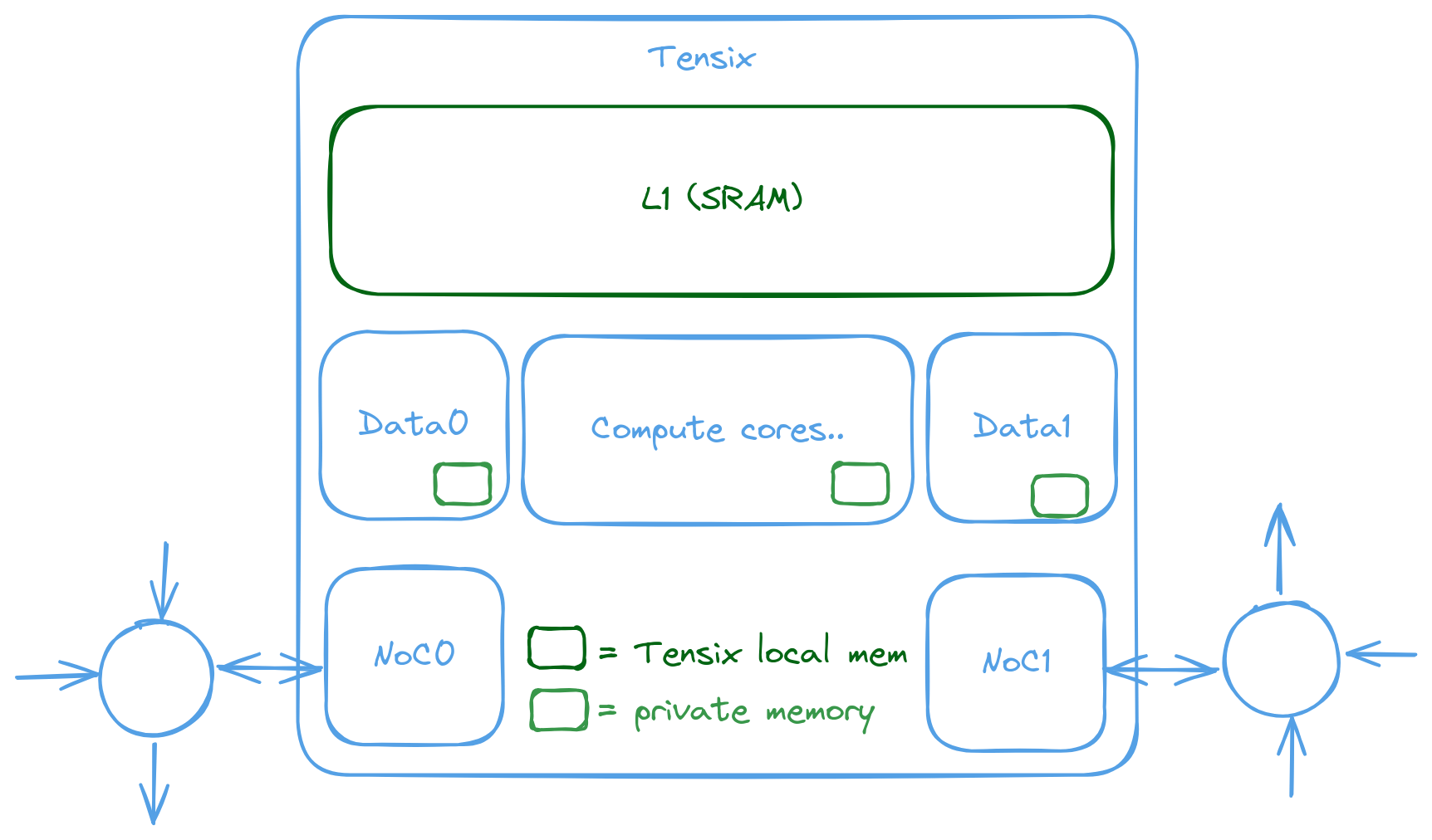
For a kernel running on data-movement core 0 of Tensix core (0, 0), the binary is placed in that core’s shared SRAM (historically “L1”). At runtime, instructions stream from shared SRAM into a small per-core instruction cache (0.5-2 KiB, about 128-512 instructions) to cut repeated SRAM fetches. Each RISC-V core also has a small private memory region for its stack and locals; this region and the shared SRAM are mapped at identical addresses on every core. The shared SRAM is always accessible to all cores; only the private region is isolated. Because many on-core agents contend for shared SRAM, RISC-V loads and stores to it have limited bandwidth and a latency of several cycles.
Refer to the Baby RISC-V documentation for the RISC-V address space. The L1 page documents the shared SRAM (L1) organization, its clients and performance characteristics.
// the function (machine code) lives on L1. When executed, a 0.5~2KiB
// instruction cache (depending on which core is selected) reduces
// SRAM access pressure
void kernel_main() {
    int a = 0; // lives on per-core private memory
    // Because of this, passing the address of this variable to another core
    // will not work, as the other core does not have access to the private memory
    // it lives on. And has the core has its own private memory mapped at the same address

    // Variable `cb_idx` lives in per-core memory but points to a circular buffer in shared SRAM
    // Because shared SRAM is mapped in the core's address space, you can cast it to a pointer
    // and access it as if it were a regular memory.
    // However note that the RISC-V cores itself have low bandwidth to SRAM, the bulk of compute
    // is done via peripherals which have much higher bandwidth to SRAM.
    cb_wait_front(tt::CBIndex::c_16, 1);
    uint32_t cb_addr = get_write_ptr(tt::CBIndex::c_16);
    // Treating it as address because the address is in shared SRAM
    // DPRINT("Value at circular buffer: {}\n", ((uint32_t*)cb_addr)[0]);

    // `dram_addr` is a DRAM address, however the address is not mapped in the RISC-V address space
    // and the content must be explicitly fetched from DRAM using NoC APIs and requesting a transfer
    uint32_t dram_addr = get_arg_val<uint32_t>(0);
}
The memory blocks and related peripherals within the Tensix core can be visualized with the following diagram. Compute-related blocks are not shown as they are consumers of the memory system rather than part of the memory hierarchy discussed here.
DRAM tiles
Tensix tiles are one type of tile on the NoC. Each Tensix tile contains 1.5MB of SRAM. DRAM tiles, in contrast, connect to memory controllers that interface with off-chip GDDR memory. This provides significantly more storage capacity but with higher latency and lower bandwidth compared to SRAM.
For example, Wormhole has 6 DRAM controllers, each connected to 2GB of GDDR6 memory (2 channels, 1GB per channel). The following image shows Wormhole’s NoC grid with DRAM tiles labeled D1 to D6, corresponding to controllers 1-6. Multiple DRAM tiles can connect to the same controller to improve NoC connectivity. The DRAM tile placement is optimized for physical routing constraints rather than uniform distribution.
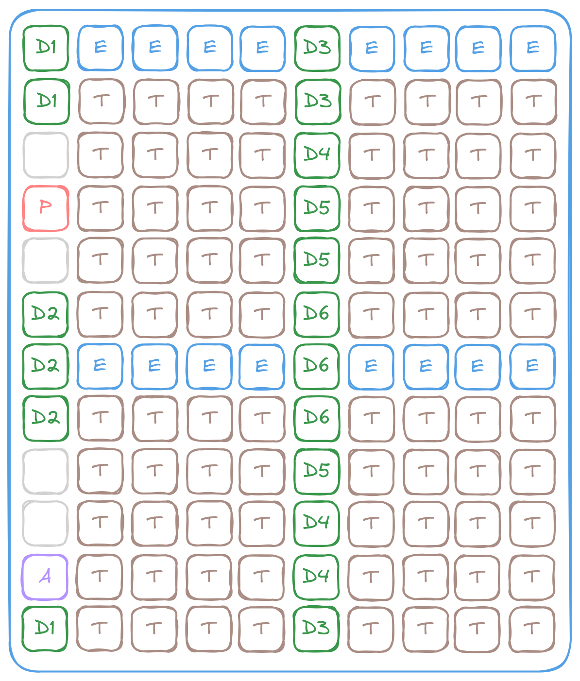
The NoC grid of the Tenstorrent Wormhole processor (D = DRAM, T = Tensix, E = Ethernet, A = ARC/management, P = PCIe).
For Wormhole, within each DRAM tile, the 1st channel is mapped to address 0 and the 2nd channel is mapped from address 1GB.
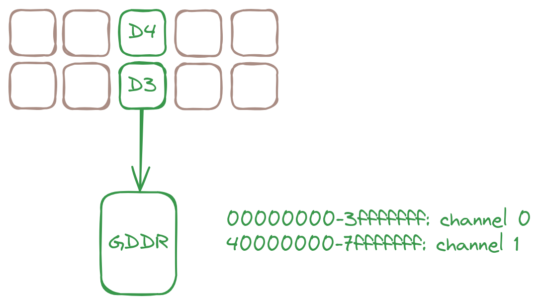
The DRAM tile connection to GDDR memory. Each DRAM tile has 2 channels, each with 1GB of memory.
Memory access via the NoC
RISC-V cores can only access their private memory and the local shared SRAM directly. Accessing SRAM on other Tensix cores or DRAM requires sending DMA requests through the NoC. These requests specify the target tile’s (x, y) coordinates and the address within that tile.
uint64_t noc_addr = get_noc_addr(x, y, addr_on_target_tile);
noc_async_read(noc_addr, ptr_l1_buffer, dram_buffer_size);

// for writing
noc_async_write(ptr_l1_buffer, noc_addr, dram_buffer_size);
Warning
Private memory (including the stack) is only accessible by the core that owns it. NoC requests can only access shared SRAM addresses:
Stack variables cannot be used as DMA source or destination
L1 buffers (allocated in the host program) and circular buffers are accessible via NoC
e.g. The following will not work.
// This WILL NOT work as arr lives on the stack which is private to the core
int arr[8];
noc_async_read(noc_addr, uint32_t(&arr), sizeof(arr));
The same scheme works for all tiles on the NoC (as long as the address maps to valid memory). If the NoC request goes to a Tensix or Ethernet tile, it accesses their SRAM; if to a DRAM tile, it accesses DRAM; to the PCIe controller, it accesses the peripheral. Thus making the real address a tuple of (x, y, local_addr).
Accessing raw DRAM is straightforward. The following creates a read request of size 0x100 to DRAM tile D1 at address 0x1000:
uint64_t noc_addr = get_noc_addr_from_bank_id<true>(0, 0x1000);
noc_async_read(noc_addr, ptr_l1_buffer, 0x100);
From the information above, the following is true on Wormhole (and analogous for other generation of processors):
All 3 D1 tiles are connected to the same DRAM controller
Reading from different D1 tiles at the same address returns the same data
Address 0x1000 is within the first 1GB, so the 1st channel of the GDDR chip is used
Using all 6 DRAM controllers simultaneously provides the full 12GB capacity
As the async naming in noc_async_read/write indicates. NoC requests are asynchronous, may complete out of order, and may or may not return immediately due to various factors. A barrier is needed to ensure that all read or write operations are complete before proceeding.
noc_async_read_barrier(); // Wait for all read operations to complete
noc_async_write_barrier(); // Wait for all write operations to complete
Tensor Layout
Tensors are the primary data structure that Metalium is designed to work with, though they are not strictly the only supported data structure. Tensors are multi-dimensional arrays used to represent various types of data, from images to text. As the fundamental data structure in modern machine learning frameworks, tensors provide flexibility and power for diverse computational tasks. Metalium is designed to facilitate efficient tensor operations.
Multiple tensor memory layouts exist, with traditional systems using either C-style row-major or Fortran-style column-major ordering. Metalium supports C-style row-major ordering but uses a custom tiled layout for optimal computation performance on the Tensix core. This tiled layout reduces silicon area, power consumption, and memory bandwidth by matching the Tensix core’s compute units and memory architecture.
Due to the lack of a linear, flat address space, data placement (onto each memory resource) requires explicit decisions about distribution and chunk size. Distribution will be discussed in a future section. The chunk size, or the amount of data stored before switching to the next storage location, is referred to as the page size.
In row-major layout, a single row of the tensor occupies one page, enabling simpler programming and lower logic overhead for common patterns of data access.
The row-major memory layout of a tensor. The data is stored in a single contiguous block of memory, with the last dimension varying the fastest.
In contrast, the tiled layout provides optimal performance for computations on the Tensix core. It divides the tensor into smaller tiles, typically 2D tiles of size 32x32 (padded as needed). Each tile is stored in a separate page, enabling efficient access patterns that align with the Tensix core’s internal compute units. See Tile documentation for details on the tile layout and its implications.
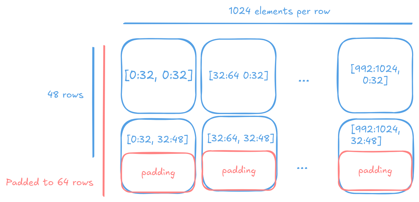
The tiled memory layout of a tensor.
Memory placement
Due to the lack of a single linear address space, data placement requires explicit decisions about location and distribution across available resources. The following factors determine optimal data placement:
Target tile selection: Which specific tile should store each piece of data
Memory type: Whether data should reside in DRAM or SRAM based on access patterns and capacity requirements
Access pattern optimization: Minimizing NoC traffic by placing frequently accessed data close to consuming cores
Compatibility across generations: Ensuring kernels can run on different Tenstorrent generations with varying memory configurations, without code changes
There is no one-size-fits-all solution for data placement. The optimal strategy depends on the specific kernel, its access patterns and the underlying hardware architecture.
Lock step allocation
Each generation of Tenstorrent processors has a different memory configuration. For example, Wormhole has 6 DRAM controllers with 2 GB each, while Blackhole has 8 controllers with 4 GB each. Passing in a separate address for each DRAM controller to a kernel is not practical nor scalable. Similarly, providing 64 addresses for each Tensix core (as on a Wormhole n150) for data residing on SRAM is not feasible.
Lock-step allocation solves this problem. For DRAM allocation, the buffer size is divided and rounded up by the number of DRAM tiles. Allocation assumes the processor has only 1/N of the total memory. The resulting address is then shared across all DRAM tiles, effectively multiplying the available space and restoring the allocated area to the requested amount. This approach ensures that a single pointer (plus the memory type, which is known before kernel execution) can uniquely identify an object, regardless of the underlying memory configuration. The same applies to SRAM allocation, where the address is shared across all Tensix cores.
The lock-step where single address can be used across multiple DRAM tiles. At the cost of some memory waste.
Lock step allocation has inherent trade-offs. When allocating X bytes on one DRAM controller, all other controllers must reserve the same amount. Additionally, if the allocation size is not evenly divisible by the number of controllers, some banks will contain unused space. Despite these limitations, the programming model simplification justifies the overhead - kernels receive a single address parameter instead of N hardware-dependent pointers, at the cost of some memory waste and explicit specification of the storage pattern.
Interleaved memory
Interleaved is the simplest memory placement scheme. Data is round‑robined across all available memory resources at page_size granularity. This approach is the most generic and works well for most kernels. It ensures that data is evenly distributed across all memory banks and not hot-spotted on any single one. At the cost of less efficient memory access patterns for certain operations such as matrix multiplication and convolution, where locality is paramount.
The following example is a typical interleaved memory allocation for a DRAM buffer. It allocates a buffer of size tile_size_bytes * n_tiles bytes. The page_size is set to the size of a tile, which 2KiB for bfloat16 tiles - each DRAM controller will hold a tile of data, and the next tile will be stored on the next DRAM controller, and so on.
constexpr uint32_t n_tiles = 64;
constexpr uint32_t elements_per_tile = tt::constants::TILE_WIDTH * tt::constants::TILE_HEIGHT;
constexpr uint32_t tile_size_bytes = sizeof(bfloat16) * elements_per_tile;

tt_metal::InterleavedBufferConfig dram_config{
    .device = device,
    .size = tile_size_bytes * n_tiles,
    .page_size = tile_size_bytes,
    .buffer_type = tt_metal::BufferType::DRAM};

auto src0_dram_buffer = CreateBuffer(dram_config);
auto in0_addr = src0_dram_buffer->address();

// Tell the kernel how to access the memory
std::vector<uint32_t> compile_time_args; // passed to kernel during kernel setup
TensorAccessorArgs(*src0_dram_buffer).append_to(compile_time_args);
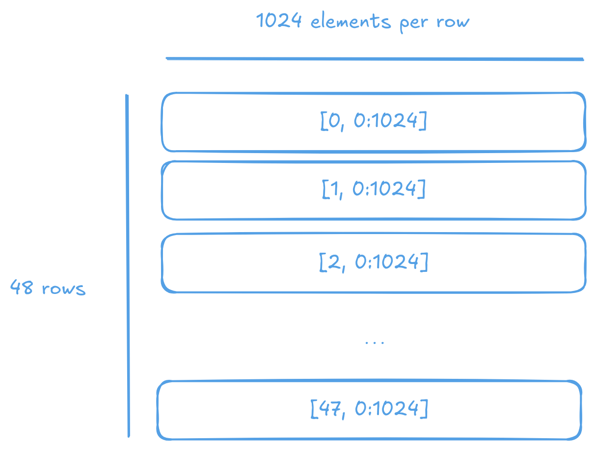
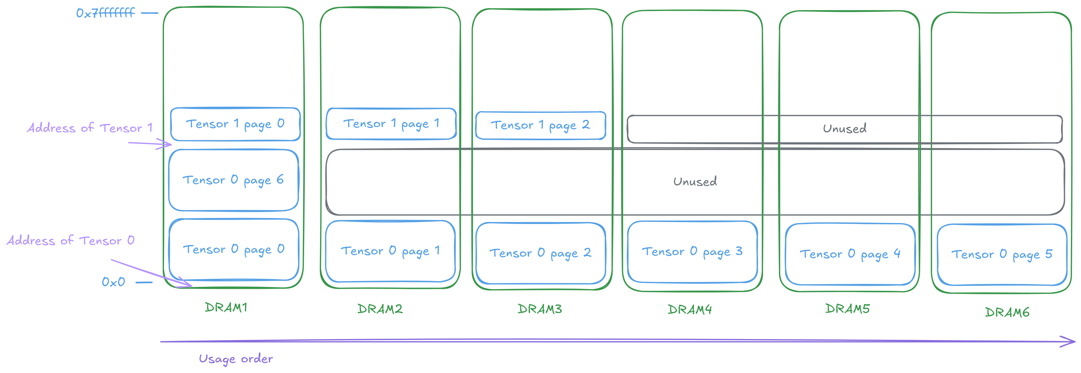
The above code allocates 64 tiles of size 2KiB each, for a total of 128KiB. Across DRAM controllers. We can visualize the allocation (as a 1D array) as follows:
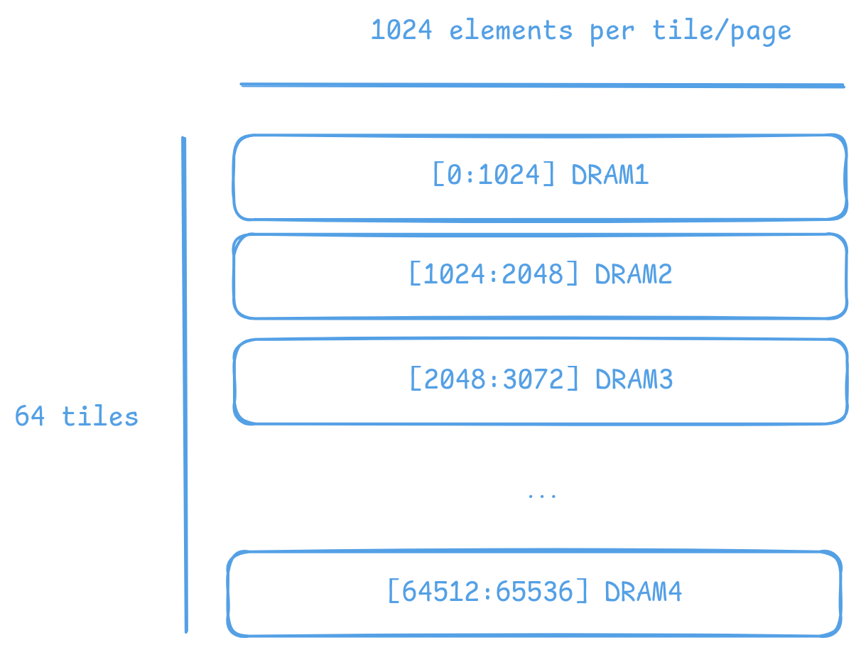
Allocation of 64 tiles of bfloat16 in interleaved memory on Wormhole (6 DRAM controllers). Each tile is 1024 elements of bfloat16, or 2KiB. The allocation round-robins across the 6 DRAM controllers.
As interleaved memory is the most common allocation scheme. Instead of manually calculating the address and tile coordinates, utilities are provided to enable easy access. TensorAccessor enables efficient, random access to interleaved memory. Allowing tile/page sized granularity for read and writes.
// access parameters are passed in compile time, starting from parameter 0
constexpr auto in0_args = TensorAccessorArgs<0>();
const auto in0 = TensorAccessor(in0_args, in0_addr, tile_size_bytes);
...

for (uint32_t i = 0; i < n_tiles; i++) {
    cb_reserve_back(cb_in0, 1);
    uint32_t cb_in0_addr = get_write_ptr(cb_in0);
    noc_async_read_page(i, in0, cb_in0_addr); // read the i-th tile from the interleaved buffer

    noc_async_read_barrier();
    cb_push_back(cb_in0, 1);
}
SRAM buffers
It is also possible to allocate buffers in SRAM. This is useful for small buffers that need to be accessed with high bandwidth, low latency and high locality. SRAM provides much higher bandwidth and lower latency than DRAM, making it ideal for intermediate data that needs to be accessed frequently during computation. However, SRAM is a very limited resource, so it is important to use it wisely and deallocate as soon as it is no longer needed.
Allocating on SRAM is exactly the same as allocating on DRAM, except that the buffer type is set to BufferType::L1. The following example allocates the same buffer as above, but in SRAM instead of DRAM. In this case, the round-robin allocation is done across all Tensix cores instead of DRAM controllers.
tt_metal::InterleavedBufferConfig sram_config{
    .device = device,
    .size = tile_size_bytes * n_tiles,
    .page_size = tile_size_bytes,
    .buffer_type = tt_metal::BufferType::L1}; // change here

auto src0_sram_buffer = CreateBuffer(sram_config);
auto in0_addr = src0_sram_buffer->address();

std::vector<uint32_t> compile_time_args;
// The knowledge that the buffer lives on SRAM is captured
TensorAccessorArgs(*src0_sram_buffer).append_to(compile_time_args);
As allocation type and scheme is known at compile time. The same TensorAccessor helper can be used to access the SRAM buffer with 0 change to the kernel.
// Nothing changes compared to reading from DRAM as allocation on DRAM or SRAM is known before
// kernel compilation.
// Whether accessing DRAM or SRAM is stored in TensorAccessorArgs.
constexpr auto in0_args = TensorAccessorArgs<0>();
const auto in0 = TensorAccessor(in0_args, in0_addr, tile_size_bytes);
...

for (uint32_t i = 0; i < n_tiles; i++) {
    cb_reserve_back(cb_in0, 1);
    uint32_t cb_in0_addr = get_write_ptr(cb_in0);
    noc_async_read_page(i, in0, cb_in0_addr);

    noc_async_read_barrier();
    cb_push_back(cb_in0, 1);
}
Sharded tensor
Interleaved memory, while simple and generic, does not always provide optimal performance for all kernels. It can lead to NoC contention since each link can only carry one packet at a time. When multiple packets attempt to traverse the same link, one must wait, causing delays and reduced throughput. The problem is true for both Interleaved DRAM and SRAM buffers. This is particularly problematic for high-bandwidth kernels with predictable access patterns, such as matrix multiplication or convolution. In these cases, more advanced memory allocation schemes that reduce contention and improve data locality often provide better performance.
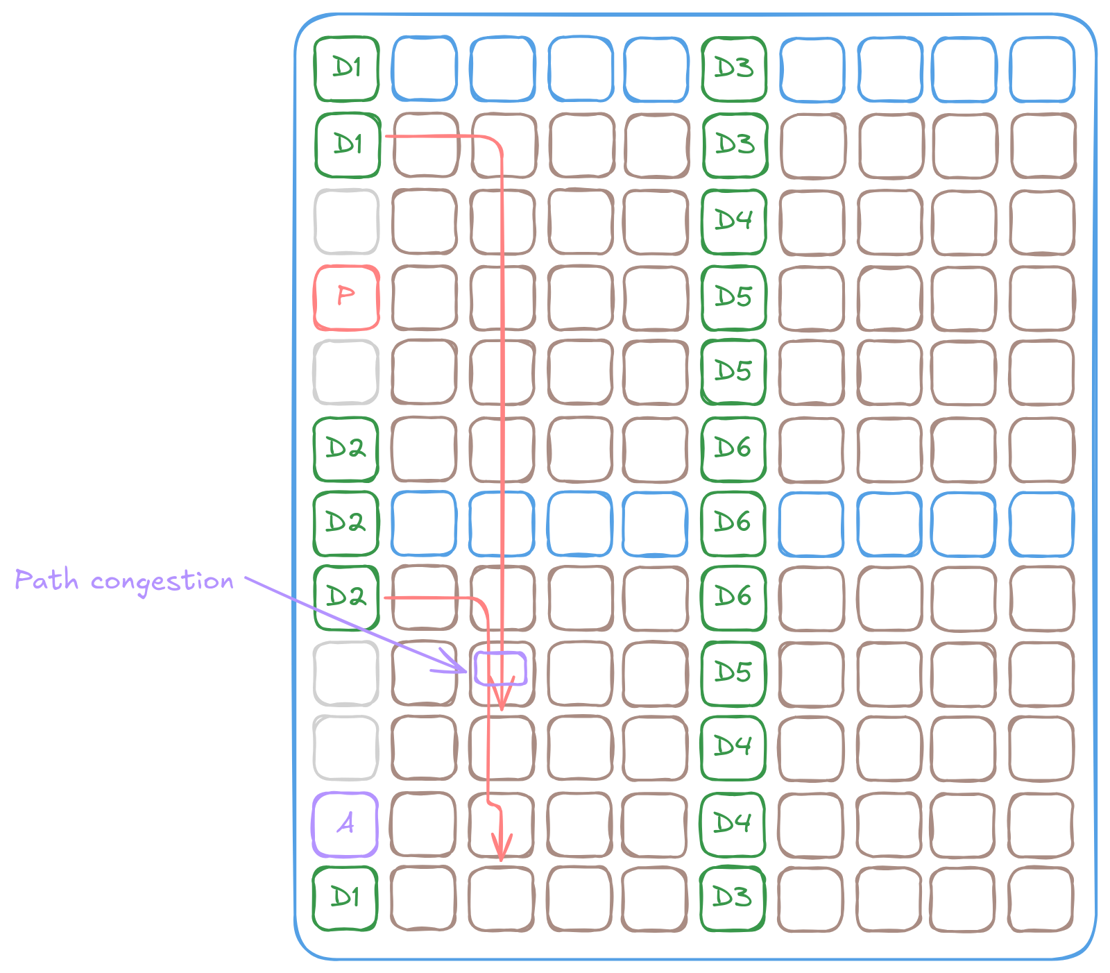
It is possible to have contention on the NoC when multiple packets try to traverse the same link.
Sharded memory is a more advanced allocation scheme that allows for, but not necessarily makes, a more efficient memory access pattern. It is used for kernels that require more control over data placement and access patterns. Sharded memory allows you to specify which tiles should store which data, and how the data should be partitioned across those tiles.
Metalium supports several sharding schemes:
Height sharding: Data is partitioned across tiles based on the height dimension
Width sharding: Data is partitioned across tiles based on the width dimension
Block sharding: Data is partitioned across tiles on both width and height dimensions
Sharding is usually only done for SRAM buffers.
using namespace tt::constants;
ShardSpecBuffer shard_spec(
    cores,                                            // The core grid on which data is distributed on
    { uint32_t(tiles_per_core_width * TILE_HEIGHT),   // Width and height in bytes
      uint32_t(tiles_per_core_height * TILE_WIDTH) },
    ShardOrientation::ROW_MAJOR,                      // direction (across cores) to distribute shards
    { TILE_HEIGHT, TILE_WIDTH },                      // Page size in elements
    { height_tiles, width_tiles });                   // shape of the overall matrix/tensor in shards

// Allocate a sharded buffer in L1
auto buf = CreateBuffer(ShardedBufferConfig{
    .device = device,
    .size = n_tiles * tile_size_bytes,
    .page_size = tile_size_bytes,
    .buffer_layout = TensorMemoryLayout::HEIGHT_SHARDED,
    .shard_parameters = shard_spec});

// Describe access pattern for kernel (compile-time args packing helper).
std::vector<uint32_t> compile_time_args;
TensorAccessorArgs(*buf).append_to(compile_time_args);
Accessing of sharded memory is done exactly like accessing interleaved memory. TensorAccessor enables efficient, random access to sharded memory. Allowing tile/page sized granularity for read and writes.
Note
Note the concepts (DRAM vs SRAM, interleaved vs sharded) are mostly independent of each other. You can have interleaved DRAM buffers (most common), interleaved SRAM buffers (often used for temporary data), sharded SRAM buffers (for specific use cases where they benefit from the bandwidth) and sharded DRAM buffers (rarely used due to limited DRAM vs NoC bandwidth thus not described above). The best approach depends on the specific kernel and its access patterns.