AXI-over-UCIe Bridge (AoU) Integration
Parameters, clocks, resets, and bring-up for the vendored AXI-over-UCIe bridge.
1. Integration guide
References
-
AXI over UCIe (AoU) Protocol Specification, v0.7 (https://cdn.sanity.io/files/jpb4ed5r/production/728b2f8cfc09023466cf350db53764890b4f2343.pdf)
-
AXI over UCIe (AoU) Protocol Specification, v0.5
-
Universal Chiplet Interconnect Express (UCIe) Specification, Revision 3.0 (https://www.uciexpress.org/)
-
Arm AMBA AXI and ACE Protocol Specification (AXI4) (https://developer.arm.com)
-
Arm AMBA APB Protocol Specification (https://developer.arm.com)
Arm, AMBA, AXI, APB, and ACE are registered trademarks or trademarks of Arm Limited (or its subsidiaries) in the US and/or elsewhere. Universal Chiplet Interconnect Express (UCIe) is a trademark of the UCIe Consortium. All other trademarks are the property of their respective owners.
Integration Options
The AOU IP can be integrated at two levels. Choose the option that matches your system's FDI bringup strategy:
| Option | Module | When to use | FDI bringup | Additional ports |
|---|---|---|---|---|
A (recommended) |
AOU_TOP |
Turn-key FDI bringup control is desired |
Handled internally by AOU_FDI_BRINGUP_CTRL |
FDI bringup control, SW bringup control, bringup status |
B |
AOU_CORE_TOP |
You have an external UCIe controller or custom FDI state machine |
Must be handled externally |
I_INT_FSM_IN_ACTIVE, O_AOU_ACTIVATE_ST_*, O_AOU_REQ_LINKRESET, O_SW_RESET |
Note: All AXI, APB, FDI datapath, interrupt, and DFT interfaces are identical between AOU_TOP and AOU_CORE_TOP. The sections below that document these interfaces apply to both modules unless otherwise noted.
For detailed micro-architecture information — including datapath internals, error handling, debugging features, and credit management — refer to the AOU_CORE Micro-Architecture Specification (DOC/MAS/index.adoc).
Module Overview
AOU_TOP
AOU_TOP is the recommended top-level integration module. It instantiates two submodules:
-
AOU_FDI_BRINGUP_CTRL — A UCIe 3.0 FDI state machine that manages the four FDI handshake pairs (wake, clock, state negotiation, RX activation) required to bring the FDI link from RESET to ACTIVE and follow LinkError, LinkReset, Disabled, Retrain, and L1 entry/exit.
-
AOU_CORE_TOP — The AXI-over-UCIe protocol engine described in AOU_CORE_TOP.
The bringup controller drives I_INT_FSM_IN_ACTIVE into the protocol engine internally, so this signal is not exposed as a top-level port on AOU_TOP. Instead, AOU_TOP exposes:
-
FDI bringup control ports for the physical layer handshakes (FDI Bringup Control Interface (AOU_TOP only))
-
Software bringup control pins (FDI Bringup Software Control (AOU_TOP only))
-
Bringup status outputs (FDI Bringup Status (AOU_TOP only))
The FDI bringup flow is described in FDI Bringup Flow (AOU_TOP only).
AOU_CORE_TOP
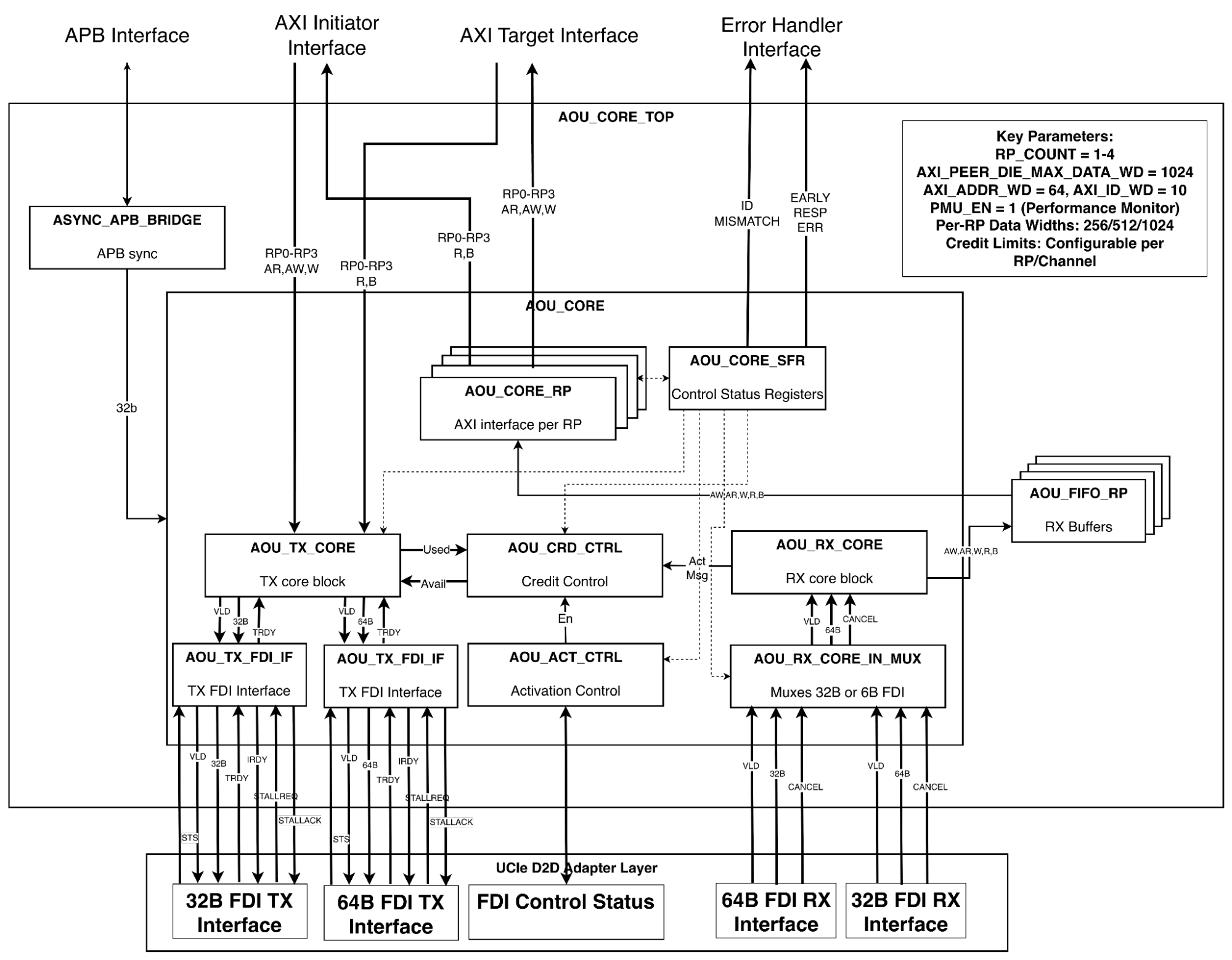
Figure 1 shows high level block diagram of AOU CORE TOP.
Purpose and Function
The AOU_CORE_TOP is a bridge between AXI interface and the UCIe FDI interface, defined in AoU standard, AXI over UCIe Protocol Specification v0.7.
To achieve low latency, AOU_CORE directly handles signals related to the UCIe FDI interface data flow control and processes data in FDI-width chunks (32, 64, or 128 bytes, as selected by the FDI_CONFIG parameter) in a cut-through manner, without converting them to 256-byte flit data. It receives AXI messages from its own AXI slave interface, packs them into FDI-width chunks, and transmits these chunks to the remote AoU device via UCIe. The remote AoU receives these FDI-width chunks from the UCIe FDI interface, unpacks them into AXI messages, and delivers the data through its AXI master interface. It supports flow control for all exceptional cases defined in the UCIe standard. First, it handles the chunk valid/cancel signal, including the alternative implementation method described in the UCIe specification. Second, it handles the stall request signal received from the D2D Adapter while maintaining the Flit-aligned boundary.
Interoperability is also supported when the remote device uses a different AXI data width. AOU_CORE supports a configurable number of Resource Plane(RPs), with both the number of RPs and each RP’s AXI data width fully parameterizable. A dedicated field in the SFR allows software to configure the target RP, enabling flexible RP mapping. The AW and AR channels are arbitrated between RPs with one of three schemes: Round Robin, AXI QoS, and Port QoS; W data follows the order of the granted AWs. Additionally, a starvation-prevention mechanism is implemented to ensure fair arbitration across all RPs.
AOU_CORE_TOP implements the subset of FDI signals required specifically for transporting AXI across UCIe. FDI bringup/teardown and FDI sideband flows are expected to be handled by other components.
The block consists of the following sub blocks
-
AOU_CORE
-
AOU_CORE_RP Manages a AXI interface for write request, read request, write data, read data and write response busses
-
AOU_CORE_SFR This implements control and status register of the AOU core. It has a 32bit APB interface for programming. It configures all the blocks in the core.
-
AOU_TX_CORE This block packs the arbitrated AXI channels, credits, and activation messages into FDI-width chunks (32, 64, or 128 bytes per FDI_CONFIG). It follows AOU specifications to pack the messages into 256 byte flit data. It then passes it onto UCIe controller over the FDI interface for transmission.
-
AOU_CRD_CTRL This block manages credits available for TX. It gets remote credits available from AOU_RX_CORE, and used credits from AOU_TX_CORE and creates final credits that can be used for TX.
-
AOU_RX_CORE This block processes FDI-width chunks (32, 64, or 128 bytes per FDI_CONFIG) received by UCIe controller and passed to the core over the FDI interface. It decodes different message types which encapsulate different AXI channel transactions. These messages are buffered and then passed onto AOU_CORE_RP for presenting the transaction to its corresponding AXI interface.
-
AOU_TX_FDI_IF This block receives FDI-width data chunks from AOU_TX_CORE and buffers them. It does handshake with UCIe controller FDI RX interface and passes the data chunks downstream to be sent to remote chiplet.
-
AOU_ACT_CTRL This block manages activation and deactivation control of the AOU bridge. It initiates activate and deactivate messages to remote AOU bridge when configured via APB.
-
-
AOU_FIFO_RP This block buffers decoded messages from AOU_RX_CORE. It separates the messages based on resource plane (RP) indicator and writes them into dedicated FIFOs. These FIFOs feed the corresponding AOU_CORE_RP which manage a single AXI interface. The FIFOs are on the core reset together with AOU_CORE (I_RESETN and AOU_CON0.AOU_SW_RESET, Reset domains).
-
ASYNC_APB_BRIDGE This block synchronizes APB transactions to the local core clock.
When using AOU_CORE_TOP directly, the integrator must provide an external FDI state machine that drives I_INT_FSM_IN_ACTIVE and the associated control/status signals listed in UCIe / External Control and Status.
Key Features
-
Single APB interface Configuration/control/status register access
-
Multiple AXI master & slave interface
-
Configurable RP port & RP remapping supported
-
Supports variable data widths and burst length requests. Configurable FIFO Depth
-
-
UCIe 256B latency-optimized flit(Format 6) support only
-
Message packing and unpacking are handled in variable-sized units of 32, 64, or 128 bytes, corresponding to the FDI data width selected by FDI_CONFIG.
-
Selectable Early response by setting SFR8
-
Selectable 32B / 64B / 128B single-PHY and 32B+64B / 64B+128B two-PHY FDI configurations via the FDI_CONFIG parameter (see Parameter List). Two-PHY variants additionally require the +define+TWO_PHY build flag so the second-PHY ports physically exist.
-
Parameterized number of Resource Plane and each RP’s AXI data width
-
RP Remapping
-
QoS scheme between RPs on the AW and AR channels
-
Interoperability with different data width remote die
-
Handling of flit cancel and stall request as specified in the UCIe specification
-
Selectable AXI Aggregator added for BUS efficiency
Parameter List
| Parameter | Type | Default / Note | Description |
|---|---|---|---|
RP_COUNT |
parameter |
1 |
Number of receive ports (AXI M/S pairs). Parameterizable up to 4. |
FDI_CONFIG |
parameter (int) |
FDI_CFG_SP_32B |
FDI width selector. See FDI_CONFIG values below. Two-PHY values additionally require +define+TWO_PHY at compile time. |
RP0_RX_AW_FIFO_DEPTH |
parameter |
44 |
RX AW FIFO depth for RP0. The depth of each RP*_RX_*_FIFO_DEPTH parameter should be determined by considering the Turn-Around-Time (TAT) between the local die and the remote die, so that no performance drop occurs due to AoU — TAT being the time, in a UCIe-integrated environment, from when the local die sends a message until the credit is received back from the remote die. |
RP0_RX_AR_FIFO_DEPTH |
parameter |
44 |
RX AR FIFO depth for RP0. |
RP0_RX_W_FIFO_DEPTH |
parameter |
88 / 140 |
RX W FIFO depth for RP0. Default is 140 when FDI_CONFIG selects a 1024b interface (FDI_CFG_SP_128B / FDI_CFG_TP_64B_128B); 88 otherwise. |
RP0_RX_R_FIFO_DEPTH |
parameter |
88 / 140 |
RX R FIFO depth for RP0. Same FDI-aware default as RP0_RX_W_FIFO_DEPTH. |
RP0_RX_B_FIFO_DEPTH |
parameter |
44 |
RX B FIFO depth for RP0. |
RP1_RX_AW_FIFO_DEPTH |
parameter |
44 |
RX AW FIFO depth for RP1. |
RP1_RX_AR_FIFO_DEPTH |
parameter |
44 |
RX AR FIFO depth for RP1. |
RP1_RX_W_FIFO_DEPTH |
parameter |
88 / 140 |
RX W FIFO depth for RP1 (FDI-aware default; see RP0). |
RP1_RX_R_FIFO_DEPTH |
parameter |
88 / 140 |
RX R FIFO depth for RP1 (FDI-aware default; see RP0). |
RP1_RX_B_FIFO_DEPTH |
parameter |
44 |
RX B FIFO depth for RP1. |
RP2_RX_AW_FIFO_DEPTH |
parameter |
44 |
RX AW FIFO depth for RP2. |
RP2_RX_AR_FIFO_DEPTH |
parameter |
44 |
RX AR FIFO depth for RP2. |
RP2_RX_W_FIFO_DEPTH |
parameter |
88 / 140 |
RX W FIFO depth for RP2 (FDI-aware default; see RP0). |
RP2_RX_R_FIFO_DEPTH |
parameter |
88 / 140 |
RX R FIFO depth for RP2 (FDI-aware default; see RP0). |
RP2_RX_B_FIFO_DEPTH |
parameter |
44 |
RX B FIFO depth for RP2. |
RP3_RX_AW_FIFO_DEPTH |
parameter |
44 |
RX AW FIFO depth for RP3. |
RP3_RX_AR_FIFO_DEPTH |
parameter |
44 |
RX AR FIFO depth for RP3. |
RP3_RX_W_FIFO_DEPTH |
parameter |
88 / 140 |
RX W FIFO depth for RP3 (FDI-aware default; see RP0). |
RP3_RX_R_FIFO_DEPTH |
parameter |
88 / 140 |
RX R FIFO depth for RP3 (FDI-aware default; see RP0). |
RP3_RX_B_FIFO_DEPTH |
parameter |
44 |
RX B FIFO depth for RP3. |
RX_AW_FIFO_RS_EN |
parameter |
1 |
When 1, inserts an output register-slice on the RX AW FIFO read port. Trades latency (+1 cycle) for timing closure. |
RX_AR_FIFO_RS_EN |
parameter |
1 |
RX AR FIFO output register-slice enable (see RX_AW_FIFO_RS_EN). |
RX_W_FIFO_RS_EN |
parameter |
1 |
RX W FIFO output register-slice enable (see RX_AW_FIFO_RS_EN). |
RX_R_FIFO_RS_EN |
parameter |
1 |
RX R FIFO output register-slice enable (see RX_AW_FIFO_RS_EN). |
RX_B_FIFO_RS_EN |
parameter |
1 |
RX B FIFO output register-slice enable (see RX_AW_FIFO_RS_EN). |
RP0_AXI_DATA_WD |
parameter |
512 |
AXI data width for RP0 (bits). |
RP1_AXI_DATA_WD |
parameter |
512 |
AXI data width for RP1 (bits). |
RP2_AXI_DATA_WD |
parameter |
512 |
AXI data width for RP2 (bits). |
RP3_AXI_DATA_WD |
parameter |
512 |
AXI data width for RP3 (bits). |
AXI_PEER_DIE_MAX_DATA_WD |
localparam |
1024 |
Width of the widest AoU data message (WriteData1024 / ReadData1024), which sizes the RX data path. The receiver cannot know the remote die’s AXI data width, so this is fixed at the AoU maximum and is not an integration parameter: AOU_CORE accepts every legal message width from any remote die. |
APB_ADDR_WD |
parameter |
32 |
APB address width. Only PADDR[15:0] is decoded (APB Slave Interface). |
APB_DATA_WD |
parameter |
32 |
APB data width. |
S_RD_MO_CNT |
parameter |
32 |
Slave read outstanding count. |
S_WR_MO_CNT |
parameter |
32 |
Slave write outstanding count. |
TX_NXT_PACKING_EN |
parameter |
0 |
TX flit packer output stage in AOU_TX_CORE. 0: each FDI chunk is driven combinationally from the granule ring and the current packing state. 1: the chunk is computed from the look-ahead (next) packing state and ring contents and registered before the FDI output mux, so the FDI TX data leaves a register. |
M_RD_MO_CNT |
parameter |
32 |
Number of remote read requests an RP keeps in service at its AXI manager port (one pending-ID table entry per request, from the first AR it issues for the request until the last R beat). A request the splitter cuts into sub-bursts (AOU_SPLIT_TR_RPn.MAX_ARBURSTLEN, AXI Transaction Splitter in DOC/MAS/architecture.adoc) holds one entry for all of them, so the manager port may have up to M_RD_MO_CNT x ceil(beats / (MAX_ARBURSTLEN + 1)) read bursts outstanding, where beats is the request’s length at the manager port’s data width. The local interconnect may back-pressure AR as usual. |
M_WR_MO_CNT |
parameter |
32 |
Number of remote write requests an RP keeps in service at its AXI manager port (one pending-ID table entry per request, from the first AW it issues for the request until the last B). As for reads, a split request holds one entry for all of its sub-bursts, so the manager port may have up to M_WR_MO_CNT x ceil(beats / (MAX_AWBURSTLEN + 1)) write bursts outstanding. |
RP0_AGG_WCH_FIFO_DEPTH … RP3_AGG_WCH_FIFO_DEPTH |
localparam in AOU_CORE_TOP (parameter of AOU_CORE) |
16 |
Depth of the per-RP W-channel FIFO that decouples AW from W inside the AXI Aggregator. It must be greater than the longest write burst the local bus issues to the AXI manager port (the aggregator issues an AW only once the FIFO can hold the whole recalculated burst). Fixed at 16 in AOU_CORE_TOP; change the localparams there to integrate a longer-burst local bus. |
FDI_CONFIG values
FDI_CONFIG is a single integer parameter that selects the FDI data width pair forwarded to the internal hierarchy. Named constants are declared in RTL/packet_def_pkg.sv and should be used at the instantiation site:
| FDI_CONFIG value | PHY0 width (FDI_IF_WD0) | PHY1 width (FDI_IF_WD1) | PHY count | Build flag |
|---|---|---|---|---|
FDI_CFG_SP_32B (default) |
256 |
512 (internal decode) |
Single PHY |
none |
FDI_CFG_SP_64B |
512 |
512 (internal decode) |
Single PHY |
none |
FDI_CFG_SP_128B |
1024 |
1024 (internal decode) |
Single PHY |
none |
FDI_CFG_TP_32B_64B |
256 |
512 |
Two PHY |
+define+TWO_PHY |
FDI_CFG_TP_64B_128B |
512 |
1024 |
Two PHY |
+define+TWO_PHY |
Notes:
-
For single-PHY values, only the PHY0 ports (I_FDI_PL_0_* / O_FDI_LP_0_*) carry traffic. The PHY1 internal width is used only as the RX-side decode width.
-
The two-PHY values (FDI_CFG_TP_*) are valid only when the design is built with +define+TWO_PHY. The build flag gates the physical presence of the PHY1 ports (I_FDI_PL_1_*, O_FDI_LP_1_*) and the I_PHY_TYPE selector on both AOU_TOP and AOU_CORE_TOP. Mixing a FDI_CFG_TP_* value with a build that omits +define+TWO_PHY (or vice-versa) is an integration error; the design does not enforce this consistency at elaboration time.
-
The FDI_CFG_TP_32B_128B (256b + 1024b) combination is not supported by the design: AOU_RX_CORE_IN_MUX requires FDI_IF_WD0 == FDI_IF_WD1 / 2 for two-PHY accumulation.
Build flags
| Flag | Effect |
|---|---|
+define+TWO_PHY |
Compile-time switch that adds the second-PHY ports (I_FDI_PL_1_*, O_FDI_LP_1_*) and the I_PHY_TYPE selector to both AOU_TOP and AOU_CORE_TOP. Required for FDI_CFG_TP_* values of FDI_CONFIG. |
Interface Signals
Clock and Reset
| Signal | Direction | Width | Description |
|---|---|---|---|
I_CLK |
input |
1 |
Core system clock (AOU_CORE and AOU_FIFO_RP). |
I_RESETN |
input |
1 |
Active-low asynchronous reset for the core clock domain. See Reset domains. |
I_PCLK |
input |
1 |
APB clock (slave side of async bridge). |
I_PRESETN |
input |
1 |
Active-low reset for the APB-clock side of the async bridge. See Reset domains. |
Reset domains
I_RESETN and I_PRESETN are independent. Each may be asserted or released on its own.
I_RESETN is the core-clock reset. It returns the protocol engine, the configuration registers, and the activation state to their reset values. The activation FSM comes out of reset DISABLED. It clears the RX FIFOs. On AOU_TOP, it returns the FDI bringup controller to Reset, so the link must be trained again. In-flight AXI transactions and an FDI flit already in progress are abandoned. Software reprograms the configuration registers, brings the link up, and runs activation again. AOU_SW_RESET is the software reset used in the LinkReset sequence (PM entry / LinkReset / LinkDisabled sequence in DOC/MAS/software-operation.adoc). It resets AOU_CORE the same way, the AXI port logic and the RX FIFOs (AOU_FIFO_RP) of every RP included, with no quiesce or drain; every configuration register returns to its reset value, the AOU_SW_RESET bit itself included, so the bit is write-only and self-clearing and the reset lasts one I_CLK cycle. Scan muxing of that path is described in TIEL_DFT_MODESCAN Usage.
AXI transactions across a reset. Either reset loses every AXI transaction in flight or queued in AOU_CORE: requests accepted on the S ports and not yet sent, bursts in progress on the S or M ports, responses owed to the local managers (for reads and writes already sent to the remote die too), responses the local subordinates present on the M ports, and writes already acknowledged with an early write response whose data has not reached the remote die. Nothing is completed with an error response, and the ports do not keep the AXI protocol across the reset: VALID can drop without a handshake, a burst can end early, a response presented to an M port is never accepted and a response owed on an S port never comes. The integrator must therefore either reset the AXI managers and subordinates attached to the AoU ports together with AOU_CORE (the same reset event; on AOU_CORE_TOP, O_SW_RESET reports the software reset, UCIe / External Control and Status), or give them a recovery mechanism that abandons the transactions outstanding towards AOU_CORE, withdraws what they present and ignores a late response. Nothing a reset lost is presented on a port after it: the RX FIFOs are emptied with the core, so no beat or response received before the reset is delivered later, and the activation that follows advertises the full FIFO depth as credit. Software restarts the lost traffic once AOU_CORE is activated again. Only the LinkReset sequence resets with traffic pending; the PM entry and LinkDisable sequences drain it first (PM entry / LinkReset / LinkDisabled sequence in DOC/MAS/software-operation.adoc).
I_PRESETN is the APB-clock reset. It resets only the APB-clock side of the asynchronous APB bridge. Configuration, activation state, AXI traffic, and the FDI link stay as they are. Assert I_PRESETN or I_RESETN only after the APB master is idle (PSEL low, with no access waiting on PREADY) and the bridge’s request/done handshake has fully returned to idle in both clock domains. Keep both clocks running and PSEL low while allowing the handshake to drain before an independent reset; master-visible completion alone is insufficient. A write still sitting in the bridge can complete after the reset and change a register that the reset just cleared.
At power-on, hold both resets asserted while I_CLK and I_PCLK are running. Start APB or AXI traffic only after both resets have been released.
APB Slave Interface
| Signal | Direction | Width | Description |
|---|---|---|---|
I_AOU_APB_SI0_PSEL |
input |
1 |
APB select. |
I_AOU_APB_SI0_PENABLE |
input |
1 |
APB enable. |
I_AOU_APB_SI0_PADDR |
input |
APB_ADDR_WD |
APB address. Only bits [15:0] are decoded. |
I_AOU_APB_SI0_PWRITE |
input |
1 |
APB write. |
I_AOU_APB_SI0_PWDATA |
input |
APB_DATA_WD |
APB write data. |
O_AOU_APB_SI0_PRDATA |
output |
APB_DATA_WD |
APB read data. |
O_AOU_APB_SI0_PREADY |
output |
1 |
APB ready. Tied high. |
O_AOU_APB_SI0_PSLVERR |
output |
1 |
APB slave error. Tied low. |
Note: AOU_CORE_SFR decodes PADDR[15:0] only; bits [APB_ADDR_WD-1:16] are ignored, so the register map (offsets 0x0000 to 0x0080) repeats at every 64 KiB within the APB window. Size the APB window for 64 KiB and let the interconnect decode the upper address bits. Within the window, an offset that is not a defined register (including a non-word-aligned address) reads as 0x00000000 and ignores writes. PREADY is tied high and PSLVERR is tied low, so every access completes in one cycle without an error, mapped or not. The interface has no PSTRB; writes are 32 bits wide.
AXI Master (RX) – AR Channel
Note: The AR and AW requests on the AXI Master (RX) ports are the remote die’s ReadReq and WriteReq messages, forwarded after data-width conversion and burst splitting. AOU_CORE_TOP does not validate them against the AXI4 rules (no burst crossing a 4 KB boundary, no burst exceeding Max_Transaction_Bytes). The system integrator must ensure that the remote die issues only AXI4-compliant requests; see Assumptions in the MAS (DOC/MAS/overview.adoc).
| Signal | Direction | Width | Description |
|---|---|---|---|
O_AOU_RX_AXI_M_ARID |
output |
[RP_COUNT-1:0][AXI_ID_WD-1:0] |
Read address ID. |
O_AOU_RX_AXI_M_ARADDR |
output |
[RP_COUNT-1:0][AXI_ADDR_WD-1:0] |
Read address. |
O_AOU_RX_AXI_M_ARLEN |
output |
[RP_COUNT-1:0][AXI_LEN_WD-1:0] |
Burst length. |
O_AOU_RX_AXI_M_ARSIZE |
output |
[RP_COUNT-1:0][2:0] |
Transfer size. |
O_AOU_RX_AXI_M_ARBURST |
output |
[RP_COUNT-1:0][1:0] |
Burst type. |
O_AOU_RX_AXI_M_ARLOCK |
output |
[RP_COUNT-1:0] |
Lock. |
O_AOU_RX_AXI_M_ARCACHE |
output |
[RP_COUNT-1:0][3:0] |
Cache attributes. |
O_AOU_RX_AXI_M_ARPROT |
output |
[RP_COUNT-1:0][2:0] |
Protection. |
O_AOU_RX_AXI_M_ARQOS |
output |
[RP_COUNT-1:0][3:0] |
QoS. |
O_AOU_RX_AXI_M_ARVALID |
output |
[RP_COUNT-1:0] |
AR valid. |
I_AOU_RX_AXI_M_ARREADY |
input |
[RP_COUNT-1:0] |
AR ready. |
AXI Master (RX) – R Channel
| Signal | Direction | Width | Description |
|---|---|---|---|
I_AOU_TX_AXI_M_RID |
input |
[RP_COUNT-1:0][AXI_ID_WD-1:0] |
Read data ID. |
I_AOU_TX_AXI_M_RDATA |
input |
[RP_COUNT-1:0][RP_AXI_DATA_WD_MAX-1:0] |
Read data. |
I_AOU_TX_AXI_M_RRESP |
input |
[RP_COUNT-1:0][1:0] |
Read response. |
I_AOU_TX_AXI_M_RLAST |
input |
[RP_COUNT-1:0] |
Read last. |
I_AOU_TX_AXI_M_RVALID |
input |
[RP_COUNT-1:0] |
R valid. |
O_AOU_TX_AXI_M_RREADY |
output |
[RP_COUNT-1:0] |
R ready. |
AXI Master (RX) – AW Channel
| Signal | Direction | Width | Description |
|---|---|---|---|
O_AOU_RX_AXI_M_AWID |
output |
[RP_COUNT-1:0][AXI_ID_WD-1:0] |
Write address ID. |
O_AOU_RX_AXI_M_AWADDR |
output |
[RP_COUNT-1:0][AXI_ADDR_WD-1:0] |
Write address. |
O_AOU_RX_AXI_M_AWLEN |
output |
[RP_COUNT-1:0][AXI_LEN_WD-1:0] |
Burst length. |
O_AOU_RX_AXI_M_AWSIZE |
output |
[RP_COUNT-1:0][2:0] |
Transfer size. |
O_AOU_RX_AXI_M_AWBURST |
output |
[RP_COUNT-1:0][1:0] |
Burst type. |
O_AOU_RX_AXI_M_AWLOCK |
output |
[RP_COUNT-1:0] |
Lock. |
O_AOU_RX_AXI_M_AWCACHE |
output |
[RP_COUNT-1:0][3:0] |
Cache attributes. |
O_AOU_RX_AXI_M_AWPROT |
output |
[RP_COUNT-1:0][2:0] |
Protection. |
O_AOU_RX_AXI_M_AWQOS |
output |
[RP_COUNT-1:0][3:0] |
QoS. |
O_AOU_RX_AXI_M_AWVALID |
output |
[RP_COUNT-1:0] |
AW valid. |
I_AOU_RX_AXI_M_AWREADY |
input |
[RP_COUNT-1:0] |
AW ready. |
AXI Master (RX) – W and B Channels
| Signal | Direction | Width | Description |
|---|---|---|---|
O_AOU_RX_AXI_M_WDATA |
output |
[RP_COUNT-1:0][RP_AXI_DATA_WD_MAX-1:0] |
Write data. |
O_AOU_RX_AXI_M_WSTRB |
output |
[RP_COUNT-1:0][RP_AXI_STRB_WD_MAX-1:0] |
Write strobe. |
O_AOU_RX_AXI_M_WLAST |
output |
[RP_COUNT-1:0] |
Write last. |
O_AOU_RX_AXI_M_WVALID |
output |
[RP_COUNT-1:0] |
W valid. |
I_AOU_RX_AXI_M_WREADY |
input |
[RP_COUNT-1:0] |
W ready. |
I_AOU_TX_AXI_M_BID |
input |
[RP_COUNT-1:0][AXI_ID_WD-1:0] |
Write response ID. |
I_AOU_TX_AXI_M_BRESP |
input |
[RP_COUNT-1:0][1:0] |
Write response. |
I_AOU_TX_AXI_M_BVALID |
input |
[RP_COUNT-1:0] |
B valid. |
O_AOU_TX_AXI_M_BREADY |
output |
[RP_COUNT-1:0] |
B ready. |
AXI Slave (TX) – AR Channel
| Signal | Direction | Width | Description |
|---|---|---|---|
I_AOU_TX_AXI_S_ARID |
input |
[RP_COUNT-1:0][AXI_ID_WD-1:0] |
Read address ID. |
I_AOU_TX_AXI_S_ARADDR |
input |
[RP_COUNT-1:0][AXI_ADDR_WD-1:0] |
Read address. |
I_AOU_TX_AXI_S_ARLEN |
input |
[RP_COUNT-1:0][AXI_LEN_WD-1:0] |
Burst length. |
I_AOU_TX_AXI_S_ARSIZE |
input |
[RP_COUNT-1:0][2:0] |
Transfer size. |
I_AOU_TX_AXI_S_ARBURST |
input |
[RP_COUNT-1:0][1:0] |
Burst type. |
I_AOU_TX_AXI_S_ARLOCK |
input |
[RP_COUNT-1:0] |
Lock. |
I_AOU_TX_AXI_S_ARCACHE |
input |
[RP_COUNT-1:0][3:0] |
Cache attributes. |
I_AOU_TX_AXI_S_ARPROT |
input |
[RP_COUNT-1:0][2:0] |
Protection. |
I_AOU_TX_AXI_S_ARQOS |
input |
[RP_COUNT-1:0][3:0] |
QoS. |
I_AOU_TX_AXI_S_ARVALID |
input |
[RP_COUNT-1:0] |
AR valid. |
O_AOU_TX_AXI_S_ARREADY |
output |
[RP_COUNT-1:0] |
AR ready. |
AXI Slave (TX) – R Channel
| Signal | Direction | Width | Description |
|---|---|---|---|
O_AOU_RX_AXI_S_RID |
output |
[RP_COUNT-1:0][AXI_ID_WD-1:0] |
Read data ID. |
O_AOU_RX_AXI_S_RDATA |
output |
[RP_COUNT-1:0][RP_AXI_DATA_WD_MAX-1:0] |
Read data. |
O_AOU_RX_AXI_S_RRESP |
output |
[RP_COUNT-1:0][1:0] |
Read response. |
O_AOU_RX_AXI_S_RLAST |
output |
[RP_COUNT-1:0] |
Read last. |
O_AOU_RX_AXI_S_RVALID |
output |
[RP_COUNT-1:0] |
R valid. |
I_AOU_RX_AXI_S_RREADY |
input |
[RP_COUNT-1:0] |
R ready. |
AXI Slave (TX) – AW, W, B Channels
| Signal | Direction | Width | Description |
|---|---|---|---|
I_AOU_TX_AXI_S_AWID |
input |
[RP_COUNT-1:0][AXI_ID_WD-1:0] |
Write address ID. |
I_AOU_TX_AXI_S_AWADDR |
input |
[RP_COUNT-1:0][AXI_ADDR_WD-1:0] |
Write address. |
I_AOU_TX_AXI_S_AWLEN |
input |
[RP_COUNT-1:0][AXI_LEN_WD-1:0] |
Burst length. |
I_AOU_TX_AXI_S_AWSIZE |
input |
[RP_COUNT-1:0][2:0] |
Transfer size. |
I_AOU_TX_AXI_S_AWBURST |
input |
[RP_COUNT-1:0][1:0] |
Burst type. |
I_AOU_TX_AXI_S_AWLOCK |
input |
[RP_COUNT-1:0] |
Lock. |
I_AOU_TX_AXI_S_AWCACHE |
input |
[RP_COUNT-1:0][3:0] |
Cache attributes. |
I_AOU_TX_AXI_S_AWPROT |
input |
[RP_COUNT-1:0][2:0] |
Protection. |
I_AOU_TX_AXI_S_AWQOS |
input |
[RP_COUNT-1:0][3:0] |
QoS. |
I_AOU_TX_AXI_S_AWVALID |
input |
[RP_COUNT-1:0] |
AW valid. |
O_AOU_TX_AXI_S_AWREADY |
output |
[RP_COUNT-1:0] |
AW ready. |
I_AOU_TX_AXI_S_WDATA |
input |
[RP_COUNT-1:0][RP_AXI_DATA_WD_MAX-1:0] |
Write data. |
I_AOU_TX_AXI_S_WSTRB |
input |
[RP_COUNT-1:0][RP_AXI_STRB_WD_MAX-1:0] |
Write strobe. |
I_AOU_TX_AXI_S_WLAST |
input |
[RP_COUNT-1:0] |
Write last. |
I_AOU_TX_AXI_S_WVALID |
input |
[RP_COUNT-1:0] |
W valid. |
O_AOU_TX_AXI_S_WREADY |
output |
[RP_COUNT-1:0] |
W ready. |
O_AOU_RX_AXI_S_BID |
output |
[RP_COUNT-1:0][AXI_ID_WD-1:0] |
Write response ID. |
O_AOU_RX_AXI_S_BRESP |
output |
[RP_COUNT-1:0][1:0] |
Write response. |
O_AOU_RX_AXI_S_BVALID |
output |
[RP_COUNT-1:0] |
B valid. |
I_AOU_RX_AXI_S_BREADY |
input |
[RP_COUNT-1:0] |
B ready. |
PHY and FDI (Flit Data Interface)
The FDI port set is split into two banks: PHY0 (always present) and PHY1 (present only when the design is built with +define+TWO_PHY). Both banks use the parameterized widths derived from FDI_CONFIG (see FDI_CONFIG values).
| FDI_CONFIG | FDI_IF_WD0 (PHY0 width) | FDI_IF_WD1 (PHY1 width) | PHY1 ports present |
|---|---|---|---|
FDI_CFG_SP_32B |
256 |
512 (internal decode) |
no |
FDI_CFG_SP_64B |
512 |
512 (internal decode) |
no |
FDI_CFG_SP_128B |
1024 |
1024 (internal decode) |
no |
FDI_CFG_TP_32B_64B |
256 |
512 |
yes (+define+TWO_PHY) |
FDI_CFG_TP_64B_128B |
512 |
1024 |
yes (+define+TWO_PHY) |
PHY0 (always present)
| Signal | Direction | Width | Description |
|---|---|---|---|
I_FDI_PL_0_VALID |
input |
1 |
PHY0 flit valid from PHY. |
I_FDI_PL_0_DATA |
input |
FDI_IF_WD0 |
PHY0 flit data. |
I_FDI_PL_0_FLIT_CANCEL |
input |
1 |
PHY0 flit cancel. |
I_FDI_PL_0_TRDY |
input |
1 |
PHY0 ready. |
I_FDI_PL_0_STALLREQ |
input |
1 |
PHY0 stall request. |
I_FDI_PL_0_STATE_STS |
input |
[3:0] |
PHY0 state status. |
O_FDI_LP_0_DATA |
output |
FDI_IF_WD0 |
PHY0 flit data to PHY. |
O_FDI_LP_0_VALID |
output |
1 |
PHY0 flit valid. |
O_FDI_LP_0_IRDY |
output |
1 |
PHY0 link ready. |
O_FDI_LP_0_STALLACK |
output |
1 |
PHY0 stall acknowledge. |
PHY1 (present only when +define+TWO_PHY)
| Signal | Direction | Width | Description |
|---|---|---|---|
I_FDI_PL_1_VALID |
input |
1 |
PHY1 flit valid from PHY. |
I_FDI_PL_1_DATA |
input |
FDI_IF_WD1 |
PHY1 flit data. |
I_FDI_PL_1_FLIT_CANCEL |
input |
1 |
PHY1 flit cancel. |
I_FDI_PL_1_TRDY |
input |
1 |
PHY1 ready. |
I_FDI_PL_1_STALLREQ |
input |
1 |
PHY1 stall request. |
I_FDI_PL_1_STATE_STS |
input |
[3:0] |
PHY1 state status. |
O_FDI_LP_1_DATA |
output |
FDI_IF_WD1 |
PHY1 flit data to PHY. |
O_FDI_LP_1_VALID |
output |
1 |
PHY1 flit valid. |
O_FDI_LP_1_IRDY |
output |
1 |
PHY1 link ready. |
O_FDI_LP_1_STALLACK |
output |
1 |
PHY1 stall acknowledge. |
PHY type select (present only when +define+TWO_PHY)
| Signal | Direction | Width | Description |
|---|---|---|---|
I_PHY_TYPE |
input |
1 |
PHY selector for state-status / stall-request multiplexing: 0 = PHY0, 1 = PHY1. See PHY Type Mux. |
Interrupt and Error (to Error Handler)
| Signal | Direction | Width | Description |
|---|---|---|---|
INT_REQ_LINKRESET |
output |
1 |
Link reset request. |
INT_SI0_ID_MISMATCH |
output |
1 |
Slave interface ID mismatch. |
INT_MI0_ID_MISMATCH |
output |
1 |
Master interface ID mismatch. |
INT_EARLY_RESP_ERR |
output |
1 |
Early response error. |
INT_EARLY_WDT_ERR |
output |
1 |
Early-response write-transaction watchdog expired on an RP (see Interrupts). |
INT_FDI_LINK_DOWN |
output |
1 |
FDI link lost (I_INT_FSM_IN_ACTIVE fell) while the AoU activation FSM was in ACTIVATE, ENABLED or DEACTIVATE; the FSM returns to DISABLED (see Interrupts). |
INT_ACTIVATE_START |
output |
1 |
Activate start. |
INT_DEACTIVATE_START |
output |
1 |
Deactivate start. |
UCIe / External Control and Status
AOU_TOP users: The signals in this table are present on AOU_CORE_TOP only. When integrating via AOU_TOP, these signals are consumed/generated internally by AOU_FDI_BRINGUP_CTRL and are not exposed as top-level ports. See AOU_CORE_TOP-only Ports (not on AOU_TOP).
| Signal | Direction | Width | Description |
|---|---|---|---|
I_INT_FSM_IN_ACTIVE |
input |
1 |
FDI link established. 1 from the first Active until the link is lost (LinkError, LinkReset, Disabled, Reset); must stay 1 through Retrain and L1. Its falling edge raises INT_FDI_LINK_DOWN when the activation FSM is not DISABLED, or is DISABLED with an ActivateReq already sent or received. |
O_AOU_ACTIVATE_ST_DISABLED |
output |
1 |
Activation state disabled. |
O_AOU_ACTIVATE_ST_ENABLED |
output |
1 |
Activation state enabled. |
O_AOU_REQ_LINKRESET |
output |
1 |
AOU link reset request. |
O_SW_RESET |
output |
1 |
AOU_CON0.AOU_SW_RESET in effect: AOU_CORE is held in reset this cycle (registered). |
-
I_INT_FSM_IN_ACTIVE is an input signal that indicates that the link is established. When starting the test, I_INT_FSM_IN_ACTIVE should be 0, and when you want to activate AOU_CORE, I_INT_FSM_IN_ACTIVE should be 1. When testing with IP standalone, you must force I_INT_FSM_IN_ACTIVE. An external controller must keep it asserted through Retrain and L1 and drop it only when the link is lost (LinkError, LinkReset, Disabled, or Reset); AOU_CORE treats every falling edge while its activation FSM is not DISABLED as a link loss, returns the FSM to DISABLED and raises INT_FDI_LINK_DOWN, so a controller that drops it on every Retrain gives software that interrupt on every Retrain. This is what AOU_FDI_BRINGUP_CTRL's O_INT_FSM_IN_ACTIVE does inside AOU_TOP.
-
Bus quiescence (whether every request sent to or received from the remote die has been answered) is tracked inside AOU_CORE and reported in AOU_INIT.SLV_TR_COMPLETE / AOU_INIT.MST_TR_COMPLETE; no external BUS_CLEANY inputs exist. SLV_TR_COMPLETE also waits for the actual B responses of writes that received an early B response (WRITE_EARLY_RESPONSE_RPn.WRITE_RESP_DONE).
-
After AOU_CORE deactivation, the activation status transitions to DISABLED, allowing the UCIe link to go down. Once deactivation completes, O_AOU_ACTIVATE_ST_DISABLED is asserted to notify the UCIE_CORE.
-
When the AOU_CORE is in the ENABLED state, O_AOU_ACTIVATE_ST_ENABLED is asserted to notify the UCIE_CORE.
-
O_AOU_REQ_LINKRESET is asserted together with INT_REQ_LINKRESET when the AOU_CORE detects an AoU protocol violation, to notify the UCIE_CORE. It is a level: the sticky LP_LINKRESET status bits through their interrupt masks, held until software clears the status, and absent for a masked cause. AOU_FDI_BRINGUP_CTRL acts on it in ACTIVE and RETRAIN; raised while the link is in L1 or exiting it, the request is deferred until the link is next Active (Supported State Transitions).
-
O_SW_RESET is asserted while AOU_CON0.AOU_SW_RESET holds AOU_CORE in reset. An external FDI state machine should use it the way AOU_FDI_BRINGUP_CTRL does (Supported State Transitions): after a LinkError, AOU_CORE’s FDI data paths keep the position of the flit the LinkError interrupted until this reset, so the link must not return to Active before it has been applied.
DFT
| Signal | Direction | Width | Description |
|---|---|---|---|
TIEL_DFT_MODESCAN |
input |
1 |
Scan-mode indicator. Tie low in functional operation; assert high from the SoC scan controller during scan shift and capture. |
TIEL_DFT_MODESCAN Usage
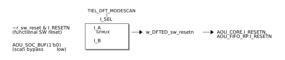
TIEL_DFT_MODESCAN controls a glitch-free mux (u_sw_reset_mux, instance of AOU_SOC_GFMUX_LVT) that selects the reset source for AOU_CORE:
-
Functional mode (TIEL_DFT_MODESCAN = 0): The mux selects I_A, the functional software-controlled reset path (~r_sw_reset & I_RESETN). This allows the CSR-writable SW reset to combine with the hardware reset.
-
Scan mode (TIEL_DFT_MODESCAN = 1): The mux selects I_B, a constant 1'b0 driven through AOU_SOC_BUF (dft_persistent_buf_scan_resetn_sw). This value de-asserts the active-low SW reset, neutralizing it so that scan chains can shift freely without the software reset logic interfering with controllability or observability.
The AOU_SOC_BUF instance exists solely to prevent the synthesis tool from optimizing away the tied-low constant; it must be preserved as a persistent buffer (see Library Cell Replacement).
The SDC file (INTEG/constraints/aou_core_top.sdc) constrains this pin with set_case_analysis 0 in functional timing mode.
Integrator DFT Responsibilities
The design provides internal DFT muxing only for the software-controlled reset path (w_DFTED_sw_resetn). The two primary hardware resets and all scan infrastructure are the integrator's responsibility:
| Responsibility | Detail |
|---|---|
HW reset DFT muxes |
I_RESETN and I_PRESETN have no internal scan-mode bypass. The integrator must add external DFT muxes (or equivalent) on both resets so they can be held inactive (high) during scan shift and capture. Without this, all flip-flops using these resets will be uncontrollable during ATPG. |
Scan chain insertion |
The design has no SCAN_EN, SCAN_IN, or SCAN_OUT ports. The integrator must insert scan chains via the synthesis tool's DFT insertion flow or by adding scan ports manually. |
Multi-clock scan definition |
I_CLK (1 GHz core) and I_PCLK (100 MHz APB) must be defined as separate scan clocks. The ATPG tool must not shift both domains simultaneously, or lockup latches must be inserted at domain boundaries. |
I/O constraints during scan |
AXI and FDI interface ports should be constrained to safe values during scan (via wrapper cells or top-level scan constraints) to prevent unintended activity on external buses. |
CDC synchronizer handling |
The AOU_SOC_SYNCHSR instances in the ASYNC_APB_BRIDGE require scan-safe treatment. See Library Cell Replacement for replacement cell requirements. |
FDI Bringup Control Interface (AOU_TOP only)
These signals connect AOU_TOP to the D2D adapter's physical layer for FDI bringup control. They are not present on AOU_CORE_TOP.
| Signal | Direction | Width | Description |
|---|---|---|---|
I_PL_INBAND_PRES |
input |
1 |
Inband presence detect from PL. The bringup FSM waits for this before initiating the wake handshake. |
I_PL_CLK_REQ |
input |
1 |
PL clock request. LP responds with O_LP_CLK_ACK. |
I_PL_WAKE_ACK |
input |
1 |
PL acknowledgement of LP wake request. |
I_PL_RX_ACTIVE_REQ |
input |
1 |
PL requests RX activation. LP responds with O_LP_RX_ACTIVE_STS. |
O_LP_STATE_REQ |
output |
[3:0] |
LP state request, UCIe encoding: NOP=0000b, Active=0001b, L1=0100b. Nothing else is requested: Retrain, L2, LinkReset and Disabled are never requested by the bringup FSM. |
O_LP_WAKE_REQ |
output |
1 |
LP-initiated wake request. |
O_LP_CLK_ACK |
output |
1 |
LP acknowledgement of PL clock request. |
O_LP_RX_ACTIVE_STS |
output |
1 |
LP RX active status in response to I_PL_RX_ACTIVE_REQ. |
O_LP_LINKERROR |
output |
1 |
LP request to take the link to LinkError (UCIe lp_linkerror). Set when the bringup FSM enters LinkError on the LP's own request (I_AOU_REQ_LINKRESET or I_SW_LINKERROR_INJECT); cleared when the PL reports LinkError or the FSM leaves LinkError. |
The four handshake pairs correspond to UCIe 3.0 FDI bringup control signals:
| Handshake | LP signal | PL signal | Purpose |
|---|---|---|---|
Wake |
O_LP_WAKE_REQ |
I_PL_WAKE_ACK |
LP-initiated link wake from low-power |
Clock |
O_LP_CLK_ACK |
I_PL_CLK_REQ |
PL-initiated clock request |
State |
O_LP_STATE_REQ |
(via I_FDI_PL_*_STATE_STS) |
State negotiation |
RX Active |
O_LP_RX_ACTIVE_STS |
I_PL_RX_ACTIVE_REQ |
RX path activation |
FDI Bringup Software Control (AOU_TOP only)
These top-level ports provide direct software control over the FDI bringup FSM. They are not SFR-mapped; the integrator must drive them from external logic or tie them as needed.
There is no software pin to take the link down or to retrain it. The bringup FSM takes the link down only for an error (via O_LP_LINKERROR). A link-down for PM entry, LinkReset or Link Disable, and the restart of the link afterwards, are done by software on the UCIe controller (D2D adapter), as described in PM Entry / LinkReset / LinkDisabled Sequence and Bringup Sequence; the FSM follows what the PL reports. UCIe does not allow the Protocol Layer to request Retrain outside Raw Format.
| Signal | Direction | Width | Description |
|---|---|---|---|
I_SW_ACTIVATE_START |
input |
1 |
Trigger FDI bringup (RESET to ACTIVE). ORed internally with the core's INT_ACTIVATE_START. |
I_SW_LINKERROR_INJECT |
input |
1 |
Force the bringup FSM into LinkError state for debug/test. Drives O_LP_LINKERROR like I_AOU_REQ_LINKRESET. |
FDI Bringup Status (AOU_TOP only)
| Signal | Direction | Width | Description |
|---|---|---|---|
O_FDI_FSM_STATE |
output |
[3:0] |
Current FDI state, in the UCIe pl_state_sts encoding: Reset=0000b, Active=0001b, L1=0100b, LinkReset=1001b, LinkError=1010b, Retrain=1011b, Disabled=1100b. The bringup states before ACTIVE (RESET, WAIT_PRESENCE, WAKE_ASSERT, WAKE_WAIT_ACK, REQ_ACTIVE) report Reset, L1 and L1_CLK_WAKE report L1, and LINKDOWN reports LinkReset or Disabled as the PL last reported. |
O_FDI_LINK_UP |
output |
1 |
Asserted when the FDI bringup FSM is in the ACTIVE state. |
AOU_CORE_TOP-only Ports (not on AOU_TOP)
The following signals are present on AOU_CORE_TOP but are not exposed on AOU_TOP. In AOU_TOP, they are consumed or generated internally by AOU_FDI_BRINGUP_CTRL.
| Signal | Direction (on AOU_CORE_TOP) | Description |
|---|---|---|
I_INT_FSM_IN_ACTIVE |
input |
FDI link established indicator. Driven by the bringup FSM's O_INT_FSM_IN_ACTIVE inside AOU_TOP: set on entry to ACTIVE, cleared on entry to LINKERROR, LINKDOWN or RESET, so 1 through RETRAIN, L1, L1_CLK_WAKE and the wake handshake that ends an L1; 0 before the first Active and after a link loss. Wider than O_FDI_LINK_UP, which is ACTIVE only. |
O_AOU_ACTIVATE_ST_DISABLED |
output |
Protocol activation state: disabled. Not used inside AOU_TOP: an AOU deactivation does not change the FDI link state. |
O_AOU_ACTIVATE_ST_ENABLED |
output |
Protocol activation state: enabled. Fed back to bringup FSM. |
O_AOU_REQ_LINKRESET |
output |
Protocol-level LinkReset request. Fed back to bringup FSM, which enters LinkError and drives O_LP_LINKERROR. |
O_SW_RESET |
output |
AOU_CON0.AOU_SW_RESET in effect. Fed back to bringup FSM, which holds the link down after a LinkError until it has been seen. |
Software operation Guide
This section gives information about operation guide for the AOU_CORE.
Register Map
The complete register map — address offsets, field definitions, access types, and reset values — is generated from the SystemRDL source and maintained separately:
-
AOU Core CSR Reference (generated from csr/aou-core.rdl)
To regenerate after editing the RDL source, see DOC/csr/README.md.
Interrupts
-
INT_ACTIVATE_START An interrupt that occurs when activation of the AoU Protocol layer is required. The interrupt can be cleared by writing '1' to the AOU_CORE.AOU_INIT.INT_ACTIVATE_START SFR.
-
INT_DEACTIVATE_START An interrupt that occurs when deactivation of the AoU Protocol layer is required. The interrupt can be cleared by writing '1' to the AOU_CORE.AOU_INIT.INT_DEACTIVATE_START SFR.
-
INT_SI0_ID_MISMATCH An interrupt that occurs on the AXI Slave Interface when a B or R channel response is received with an ID that was not previously issued as a request. Each RP’s checker is enabled by AOU_CORE.AXI_SLV_ID_MISMATCH_ERR_RPn.AXI_SLV_ID_MISMATCH_EN. Program that bit only while the activation FSM is DISABLED and no AXI traffic is outstanding on that RP. SW can check the mismatched AXI ID by reading AOU_CORE.AXI_SLV_ID_MISMATCH_ERR_RPn. The interrupt can be cleared by writing '1' to AXI_SLV_BID_MISMATCH_ERR or AXI_SLV_RID_MISMATCH_ERR.
-
INT_MI0_ID_MISMATCH An interrupt that occurs on the AXI Master Interface when a B or R channel response is received with an ID that was not previously issued as a request. SW can check the mismatched AXI ID by reading AOU_CORE.ERROR_INFO SFR. The interrupt can be cleared by writing '1' to the AOU_CORE.ERROR_INFO.SPLIT_B/RID_MISMATCH_ERR SFR.
-
INT_EARLY_RESP_ERR An interrupt that occurs when, due to the Write Early Response feature, a B response has already been sent through the AXI Slave Interface, and a subsequent actual B response arrives with an Error. SW can check the ID and error type of the transaction in which the error occurred by reading AOU_CORE.WRITE_EARLY_RESPONSE SFR. The interrupt can be cleared by writing '1' to the AOU_CORE.WRITE_EARLY_RESPONSE.WRITE_RESP_ERR SFR.
-
INT_EARLY_WDT_ERR An interrupt that occurs when the write-transaction watchdog of an RP expires: with AOU_CORE.WRITE_EARLY_RESPONSE_RPn.WDT_EN set, no AW or B handshake occurred for AOU_CORE.WRITE_EARLY_RESPONSE_WDT_CTL.WDT_THRESHOLD I_CLK cycles (reset 0xC3500) while the RP had writes outstanding, typically because the remote die stopped answering writes that already received an early OKAY. SW can find the RP by reading AOU_CORE.WRITE_EARLY_RESPONSE_RPn.WDT_TRANS_TIMEOUT_ERR; the interrupt is cleared by writing '1' to that bit and masked with AOU_CORE.AOU_INTERRUPT_MASK.INT_EARLY_WDT_MASK (bit 9). The watchdog of an RP fires once per reset: after a timeout it does not re-arm until I_RESETN or AOU_CON0.AOU_SW_RESET. See Write Transaction Watchdog in DOC/MAS/software-operation.adoc for the recovery sequence.
-
INT_REQ_LINKRESET An interrupt that occurs when AOU_CORE receives a protocol violation. Refer to the AOU_CORE Micro-Architecture Specification (DOC/MAS/interrupts-errors.adoc) for debugging details. When AOU_CORE receives a protocol violation, SW needs to do SW reset AOU_CORE and re-enter the activation sequence.
-
INT_FDI_LINK_DOWN An interrupt that occurs when the FDI link is lost while AoU is in use: I_INT_FSM_IN_ACTIVE falls (on AOU_TOP, the bringup FSM left ACTIVE for LINKERROR, LINKDOWN or RESET; Retrain and L1 do not count) while the activation FSM is in ACTIVATE, ENABLED or DEACTIVATE. The activation FSM returns to DISABLED in the same cycle and drops any handshake in flight, so no Ack timeout follows. The status bit is AOU_CORE.AOU_INIT.INT_FDI_LINK_DOWN (bit 12, write '1' to clear; cleared with the other AOU_CORE registers by AOU_CON0.AOU_SW_RESET, so the handler reads it before the reset) and the mask is AOU_CORE.AOU_INTERRUPT_MASK.INT_FDI_LINK_DOWN_MASK (bit 10; the mask gates the pin, not the status bit). Recovery is the LinkReset sequence of Link Reset SW Sequence. See Interrupt in DOC/MAS/interrupts-errors.adoc.
Activation Flow
AOU_TOP users: When using AOU_TOP, FDI bringup (RESET to ACTIVE) is handled by AOU_FDI_BRINGUP_CTRL before protocol-level activation begins. The protocol activation described in this section occurs after O_FDI_LINK_UP is asserted. See FDI Bringup Flow (AOU_TOP only) for the FDI bringup sequence.
The Activation of AOU_CORE begins after the UCIe link has been established. This is indicated by the I_INT_FSM_IN_ACTIVE signal of the AOU_CORE_TOP, which stays asserted through Retrain and L1 and falls only when the link is lost (UCIe / External Control and Status). There is no dependency between the activation of the local die and the remote die. Each die may initiate the activation sequence independently, which means the timing of sending ActivateReq can differ. Both dies must exchange ActivateReq and ActivateAck messages to transition to the ENABLED state, at which point credited messages can be transmitted.
A die sends an ActivateAck in response to an ActivateReq from the other die while its own activation FSM is DISABLED or ACTIVATE. If the local activation FSM is ENABLED, or is in DEACTIVATE, that ActivateReq is an invalid activation message (see LinkReset Error Reporting in DOC/MAS/software-operation.adoc) and is not answered: AoU specification v0.8 treats it as an inconsistent Req/Ack that moves the interface to its error state, in which nothing is transmitted (sections 8.3.3 and 8.4). It means the remote die has lost the activation state, for example because of a bug or a local reset. The local die requests LinkReset at once. Software resets AOU_CORE and both dies run activation again so they share one state.
Credit Management Type
There are two types of Credit Management Type. Since current AOU_SPEC cannot resolve pending AXI response without Activate again. When Credit Management type is set to 1, during Deactivated state, AOU_CORE can resolve pending AXI response itself.
It can be configured through AOU_CON0.CREDIT_MANAGE, and the default value is 1.
| Credit Management Type | Specification | Description |
|---|---|---|
0 |
Based on AoU v0.5 |
After deactivation, if a new request is received from the remote die, no response message can be sent. To deliver the corresponding response, the system must go through activation again after deactivation. Credit management and transmission availability for both Request-related messages and Response-related messages are controlled together. Credited messages must not be sent, after the DeactivateReq message is sent. Credits must not be sent after the DeactivateAck message is sent. The Activate Interrupt and Deactivate Interrupt that occur in the process of resuming the exchange of response messages impose mandatory requirements to set Activate and Deactivate SFR. |
1 (default) |
Proposal by BOS |
When the AoU Activity state is DEACTIVATE, manage Request-related messages (WREQ, RREQ,WDATA) and Response-related messages (RDATA, WRESP) separately. RDATA, WRESP Credited messages can be sent, after the DeactivateReq message is sent. Credits for RDATA, WRESP messages must be sent after the DeactivateAck message is sent. The Deactivate interrupt only provides a hint indicating that the remote die has started to activate / deactivate. |
Activation Start
Activation can be initiated by setting ACTIVATE_START SFR: In the current implementation, credits are granted based on the depth of the RX FIFO, so it is required to ensure that all messages in the RX FIFO are popped before sending the ActivateReq message.
Activation START (via SFR AOU_INIT.ACTIVATE_START SFR)
-
Activation can be triggered by setting ACTIVATE_START.
-
Activation does not proceed until I_INT_FSM_IN_ACTIVE is asserted, since no flits can be transmitted beforehand. Therefore, it is allowed to set the ACTIVATE_START SFR before I_INT_FSM_IN_ACTIVE is asserted. If it is set before the assertion, the activation process will automatically proceed after I_INT_FSM_IN_ACTIVE becomes asserted.
-
AOU_INIT.ACTIVATE_START SFR is automatically cleared to 0 once the activation is completed and AOU_ACTIVATE_STATE transitions to ENABLED.
Deactivation Start
Deactivation is initiated by setting the AOU_INIT.DEACTIVATE_START register. The DeactivateReq waits until the conditions in SFR setting in DOC/MAS/software-operation.adoc are met, including the DEACTIVATE_TIME_OUT_VALUE quiet window. The sequence is in the Deactivation Sequence Flow section below.
-
AOU_INIT.DEACTIVATE_TIME_OUT_VALUE is the length of a quiet window on the TX path, 2^(v + 3) core clock cycles for a programmed value v (8, 16, 32, 64, 128, 256, 512 or 1024; reset value 0 is 8). While the activation FSM is ENABLED or DEACTIVATE, the window completes after that many cycles with nothing to transmit, and it restarts when the TX path accepts or still holds a message. It is held clear in DISABLED and ACTIVATE.
-
The window may already have elapsed before software writes DEACTIVATE_START. When the TX path has been quiet for the whole window, the DeactivateReq follows the write at once; the other deactivation conditions still apply. When a message is still in the TX path, or one is accepted after the write, the DeactivateReq waits until that traffic has been gone for the full window.
-
A response the local die still has to send keeps the window open. Having received the responses to its own requests is a separate condition. When the TX path is already idle, the programmed value adds no further wait. A shorter value shortens only the wait after a message that is still in the TX path.
The ACTIVATION_OP field encodes deactivation messages as follows:
-
2 = DeactivateReq
-
3= DeactivateAck
Deactivation Sequence Flow
Once the local die issues a DeactivateReq, it can no longer provide responses to transactions initiated by the remote die. If the remote die continues to send requests or waits for responses without being notified, it may enter a hang state.
To manage this safely, the remote die must take explicit action upon receiving a DeactivateReq:
-
Immediately generate an interrupt to the CPU to inform the system software that a DeactivateReq has been received and that it must set the DEACTIVATE_START SFR. Although deactivation of the local die and the remote die operate independently, it is essential at the system level to communicate the deactivation & activation state through interrupts. This ensures that system software is explicitly informed of deactivation events and prevents the remote die from continuing to expect a response that will never arrive, thereby avoiding hang conditions.
-
This approach guarantees that once deactivation is initiated, both dies can coordinate the transition into safe and consistent DISABLED state.
-
If the software on both dies can explicitly coordinate to guarantee that all outstanding transactions have been completed and that no new transactions will be issued, then such a complicated implementation would not be necessary.
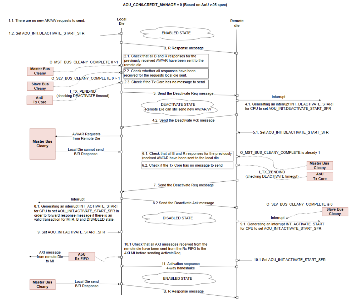
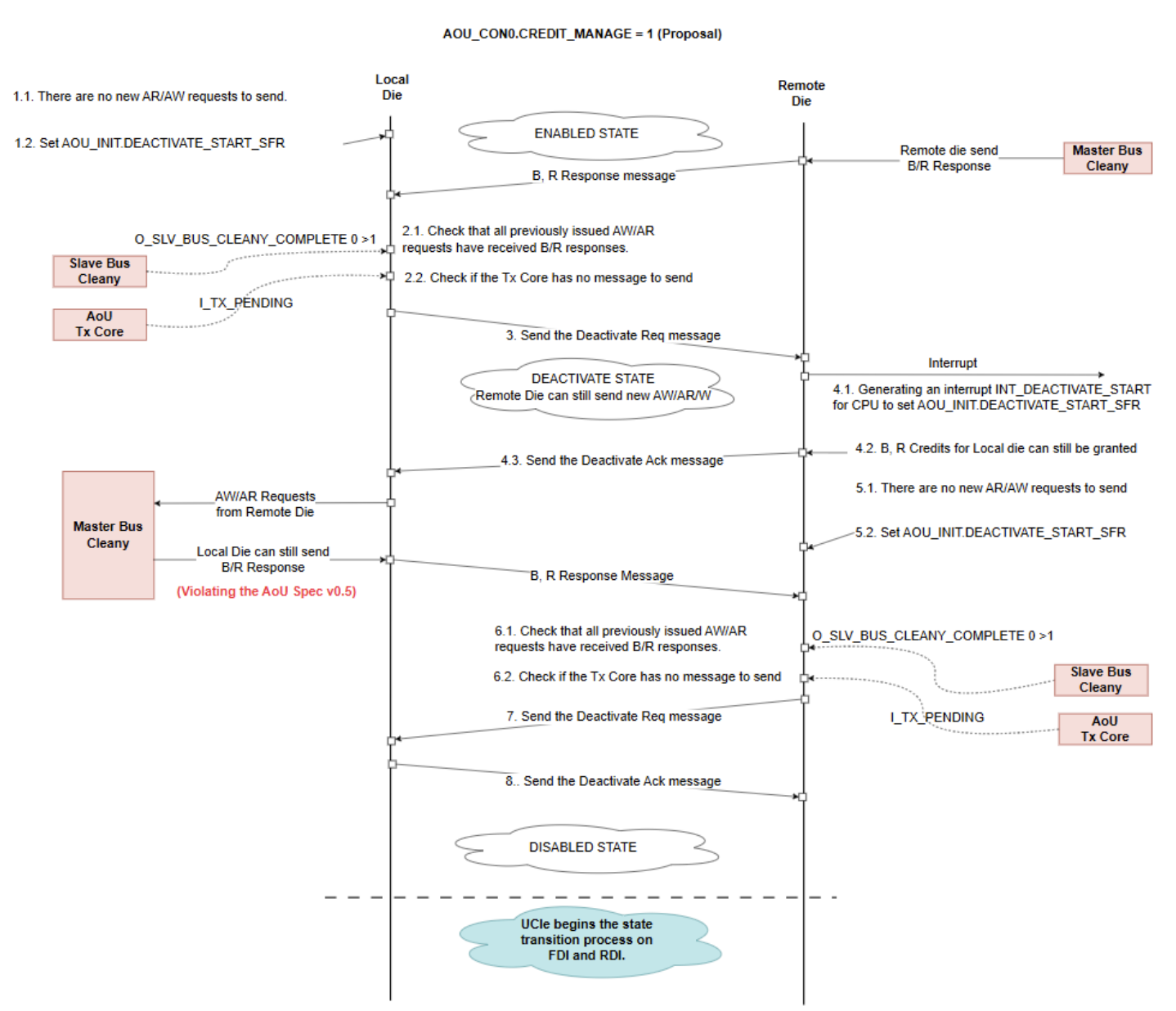
This system provides a bus cleanly-completion mechanism:
-
Slave bus cleanly indicates whether the local die has received all responses to the requests it sent to the remote die.
-
Master bus cleanly indicates whether the remote die has received all responses to the requests it sent to the local die.
After the local die sends a DeactivateReq, if the remote die issues a new request and expects a response, the system must re-enter the activation sequence before any response can be provided. Before sending a new ActivateReq, the Rx FIFO must be completely emptied – that is, all messages must be popped.
After deactivation, the credit count is reset, and during the subsequent activation process, credits are advertised based on the RX FIFO depth.
Therefore, before sending an ActivateReq, the local die must confirm, as described in the local die’s sequence 10.1, that all messages in the RX FIFO have been popped.
To meet satisfy the condition in the local die’s sequence 10.1, no backpressure must occur on the local die’s MI AW/AR/W channels.
Activation/Deactivation Interrupt
| Interrupt | Description |
|---|---|
INT_ACTIVATE_START |
When this interrupt is detected, either the AOU_INIT.ACTIVATE_START SFR must be set to 1. When AOU_INIT.ACTIVATE_STATE_ENABLED becomes 1, you must write 1 to the AOU_INIT.INT_ACTIVATE_START W1C SFR must be set to 1. An interrupt occurs when the following conditions are met while both AOU_INIT.ACTIVATE_START SFR is not set. There is a message to send When AOU_CON0.CREDIT_MANAGE is set to 0, if a new request arrives from the remote die after the local die has sent a DeactivateReq, this interrupt is asserted because the local die is required to return a response to the remote die. When AOU_CON0.CREDIT_MANAGE is set to 1, this interrupt can also be asserted if a new request after the remote die has sent a DeactivateReq. There is a response to be received (AOU_INIT.SLV_TR_COMPLETE == 0) When AOU_CON0.CREDIT_MANAGE is set to 0, this interrupt can be asserted if the local die issues new AXI requests after the remote die has sent a DeactivateReq. An ActivateReq message is received from the remote die while the activation handshake has not yet completed (DISABLED or ACTIVATE). An ActivateReq received while ENABLED is an invalid activation message and requests LinkReset, not this interrupt. See LinkReset Error Reporting in DOC/MAS/software-operation.adoc. |
INT_DEACTIVATE_START |
When AOU_CON0.CREDIT_MANAGE is set to 0, if the interrupt is detected, the master IP must stop sending new request messages and the AOU_INIT.DEACTIVATE_START SFR must be set to 1. When AOU_CON0.CREDIT_MANAGE is set to 1, if the interrupt is detected, this interrupt serves only as a hint that the remote die intends to deactivate. The local die can continue sending request messages. Once all messages have been sent, the AOU_INIT.DEACTIVATE_START SFR must be set. Otherwise, the remote die may end up in a state where it can never send requests again. When AOU_INIT.ACTIVATE_STATE_DISABLED becomes 1, SW must write 1 to the AOU_INIT.INT_DEACTIVATE_START W1C SFR must be set to 1. An interrupt can be asserted when AOU_INIT.DEACTIVATE_START SFR is not set and the local die receives a DeactivateReq message from the remote die. |
PM Entry / LinkReset / LinkDisabled Sequence
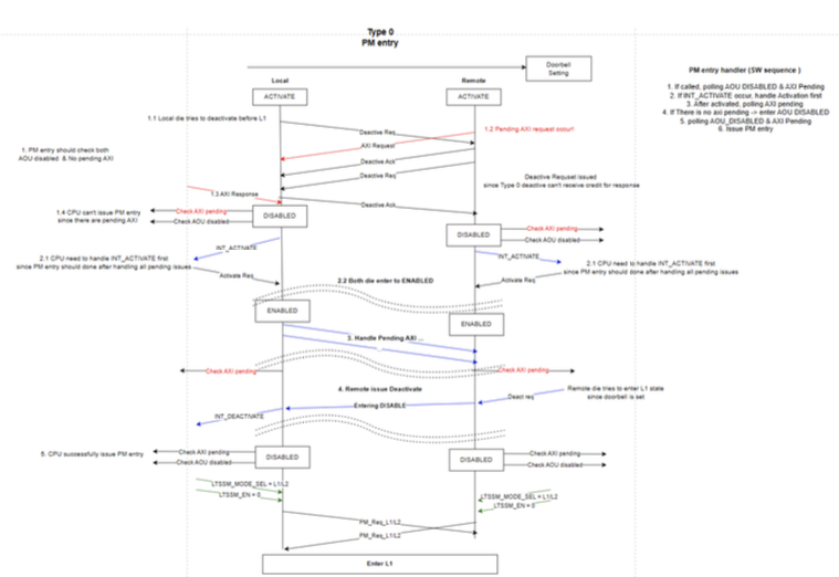
For PM entry / LinkReset / LinkDisable entry sequence, UCIE_CORE should check AOU_CORE state and try to change state. For this sequence, resolving pending AXI transactions is necessary.
Since current AOU SPEC has no way to send AXI responses after sending DeactiveReq. CREDIT_MANAGE = 0 (Type 0) is matched with current AOU_SPEC. For this case, SW needs to check whether there is pending AXI transaction.
PM Entry SW Sequence
-
Write AOU_INIT.DEACTIVATE_START to 1.
-
Polling AOU_INIT.ACTIVATE_STATE_DISABLED and AOU_INIT.SLV_TR_COMPLETE & AOU_INIT.MST_TR_COMPLETE. 2.1 Although AOU_CORE state becomes DISABLED, there may be pending AXI transactions. 2.2 AOU_CORE issues Interrupt for resolving pending AXI transactions. 2.3 Activate AOU_CORE and resolve pending AXI transactions. 2.4 Deactivate AOU_CORE
-
Polling AOU_INIT.ACTIVATE_STATE_DISABLED and AOU_INIT.SLV_TR_COMPLETE & AOU_INIT.MST_TR_COMPLETE.
-
Do PM Entry Sequence on UCIE_CORE.
Link Disable SW Sequence
Same as PM entry, before doing UCIe state transition, AOU_CORE needs to be Disabled properly.
-
Write AOU_INIT.DEACTIVATE_START to 1.
-
Polling AOU_INIT.ACTIVATE_STATE_DISABLED and AOU_INIT.SLV_TR_COMPLETE & AOU_INIT.MST_TR_COMPLETE. 2.1 Although AOU_CORE state becomes DISABLED, there may be pending AXI transactions. 2.2 AOU_CORE issues Interrupt for resolving pending AXI transactions. 2.3 Activate AOU_CORE and resolve pending AXI transactions. 2.4 Deactivate AOU_CORE
-
Polling AOU_INIT.ACTIVATE_STATE_DISABLED and AOU_INIT.SLV_TR_COMPLETE & AOU_INIT.MST_TR_COMPLETE.
-
Do LinkReset / LinkDisable Sequence on UCIE_CORE.
Link Reset SW Sequence
If AOU_CORE faces an uncorrectable error (ex. AOU SPEC violation), AOU_CORE sends LinkReset to CPU and D2D adapter. LinkReset indicates that an error has occurred which requires the Link to go down.
While handling LinkReset, SW needs to do AOU_CORE SW reset by setting AOU_CON0.AOU_SW_RESET.
Unlike the PM entry and Link Disable sequences, this one does not drain the AXI traffic first: with the link down, nothing AOU_CORE holds could complete. AOU_CON0.AOU_SW_RESET (like I_RESETN) loses every AXI transaction in flight or queued in AOU_CORE, on the S and M ports of every RP, without an error response, and the ports do not keep the AXI protocol across it. The RX FIFOs reset with the core, so nothing received before the reset is delivered after it. The AXI managers and subordinates attached to the AoU ports are reset with AOU_CORE or recover on their own, as Reset domains requires; SW restarts the lost traffic after re-activation.
SW learns of a LinkReset, Disabled or Adapter-reported LinkError that took the link down while AoU was in use from INT_FDI_LINK_DOWN (Interrupts) or from the UCIe controller; the activation FSM is already DISABLED when the handler runs. The sequence is the same: read AOU_INIT (the status bit is cleared with the other registers by AOU_CON0.AOU_SW_RESET; write '1' clears it when the handler does not reset the core), AOU_CON0.AOU_SW_RESET, restart the link on the UCIe controller, reprogram the configuration registers, ACTIVATE_START.
FDI Bringup Flow (AOU_TOP only)
This section applies only when integrating via AOU_TOP. If you are using AOU_CORE_TOP directly, you must implement an equivalent FDI state machine externally.
Overview
AOU_FDI_BRINGUP_CTRL manages the UCIe FDI state machine, handling the four handshake pairs required to bring the FDI link from RESET to ACTIVE, and follows the D2D adapter through LinkError, LinkReset, Disabled, Retrain, and L1 entry/exit. It takes the link down only for an error (O_LP_LINKERROR) and never restarts it: a link-down for PM entry, LinkReset or Link Disable, and training the link again, are done by software on the UCIe controller (Bringup Sequence). An AOU deactivation does not change the FDI link state. One sequence diagram per case (bring-up, deactivation, link-down with AoU idle and in use, LinkError from either side, Retrain, L1) is in FDI link lifecycle sequences in DOC/MAS/software-operation.adoc.
The bringup FSM operates in the I_CLK domain and uses 11 internal states: RESET, WAIT_PRESENCE, WAKE_ASSERT, WAKE_WAIT_ACK, REQ_ACTIVE, ACTIVE, RETRAIN, LINKERROR, L1, L1_CLK_WAKE and LINKDOWN. The status output O_FDI_FSM_STATE maps these to the UCIe pl_state_sts encoding (FDI Bringup Status (AOU_TOP only)).
Once the bringup FSM reaches ACTIVE, it asserts O_INT_FSM_IN_ACTIVE into AOU_CORE_TOP, which enables protocol-level activation as described in Activation Flow. The two status outputs differ on purpose: O_FDI_LINK_UP is 1 in ACTIVE only, while O_INT_FSM_IN_ACTIVE (link established) is set on entry to ACTIVE and cleared on entry to LINKERROR, LINKDOWN or RESET, so it stays 1 through RETRAIN, L1, L1_CLK_WAKE and the wake handshake that ends an L1 (WAKE_ASSERT, WAKE_WAIT_ACK, REQ_ACTIVE, which are 0 on the cold bring-up path). Its falling edge is what raises INT_FDI_LINK_DOWN in AOU_CORE when the activation FSM is not DISABLED.
Bringup Sequence
The normal (happy-path) bringup from cold reset proceeds as follows:
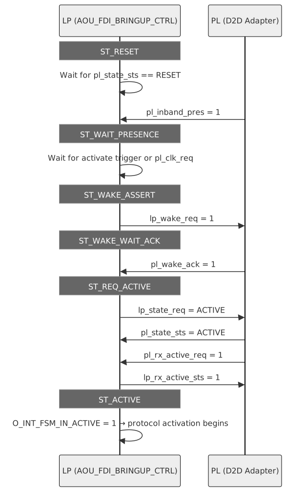
The steps in detail:
-
RESET: After hardware reset, the FSM waits for PL to report pl_state_sts = RESET and assert pl_inband_pres (remote die detected).
-
WAIT_PRESENCE: Remote die is present. The FSM asserts lp_rx_active_sts (if PL requests it) and waits for an activation trigger. The trigger can be:
-
I_SW_ACTIVATE_START (top-level port)
-
I_INT_ACTIVATE_START (from the core's activation controller)
-
I_PL_CLK_REQ (PL-initiated clock request)
-
-
WAKE_ASSERT / WAKE_WAIT_ACK: The LP-initiated wake handshake. lp_wake_req is asserted and the FSM waits for pl_wake_ack.
-
REQ_ACTIVE: Wake handshake complete. The FSM drives lp_state_req = ACTIVE and waits for both pl_state_sts = ACTIVE and pl_rx_active_req = 1.
-
ACTIVE: The FDI link is up. O_FDI_LINK_UP and O_INT_FSM_IN_ACTIVE are asserted. Protocol-level activation (Activation Flow) can now proceed. The FSM stays in ACTIVE across AOU deactivations and re-activations; it leaves only on an error or on a state change the PL reports. In RETRAIN, L1 and L1_CLK_WAKE, and through the wake handshake of an L1 exit, O_FDI_LINK_UP is 0 and O_INT_FSM_IN_ACTIVE stays 1; in LINKERROR, LINKDOWN and RESET both are 0.
After a link-down: after a LinkError (once AOU_CON0.AOU_SW_RESET has been applied, see below), or a LinkReset or Disabled the PL reports, the FSM drives lp_state_req = NOP with lp_wake_req = 0, follows the PL to Reset and waits in RESET for pl_inband_pres, exactly as after a cold reset. It gives no training trigger of its own. Software restarts the link on the UCIe controller (the D2D adapter's Start UCIe Link Training, or the remote die trains), after which pl_inband_pres rises and bringup continues from step 2 with the next activation request; software then re-activates AOU once O_FDI_LINK_UP is back. Each of these link-downs drops O_INT_FSM_IN_ACTIVE, and AOU_CORE raises INT_FDI_LINK_DOWN and returns its activation FSM to DISABLED if AoU was in use (Interrupts). An activation request seen while the FSM is in LINKERROR, LINKDOWN or RESET is dropped; the request that counts is the one seen in WAIT_PRESENCE.
Supported State Transitions
| From | To | Trigger |
|---|---|---|
Any state except LINKERROR |
LINKERROR |
pl_state_sts = LinkError |
ACTIVE, RETRAIN |
LINKERROR |
I_AOU_REQ_LINKRESET or I_SW_LINKERROR_INJECT (own request; drives O_LP_LINKERROR). Not taken in L1, L1_CLK_WAKE or the wake states: I_AOU_REQ_LINKRESET is a level and is acted on once the link is Active again (software exits L1 on the UCIe controller first); an I_SW_LINKERROR_INJECT pulse there is ignored |
Any state except LINKERROR and LINKDOWN |
LINKDOWN |
pl_state_sts = LinkReset or Disabled |
RESET |
WAIT_PRESENCE |
pl_state_sts = RESET AND pl_inband_pres = 1 |
WAIT_PRESENCE |
WAKE_ASSERT |
I_SW_ACTIVATE_START, I_INT_ACTIVATE_START or pl_clk_req = 1 |
WAIT_PRESENCE |
RESET |
pl_inband_pres = 0 |
WAKE_ASSERT |
WAKE_WAIT_ACK |
Unconditional (1 cycle) |
WAKE_WAIT_ACK |
REQ_ACTIVE |
pl_wake_ack = 1 |
WAKE_WAIT_ACK, REQ_ACTIVE |
RESET |
pl_inband_pres = 0 AND pl_state_sts = RESET |
REQ_ACTIVE |
ACTIVE |
pl_state_sts = ACTIVE AND pl_rx_active_req = 1 |
ACTIVE |
RETRAIN |
pl_state_sts = Retrain (PL-initiated only) |
ACTIVE |
L1 |
pl_state_sts = L1 (PL-initiated only) |
ACTIVE |
RESET |
pl_state_sts = RESET |
RETRAIN |
ACTIVE |
pl_state_sts = ACTIVE. RETRAIN drives lp_state_req = NOP for one cycle, then Active (the NOP to Active transition that ends a Retrain, UCIe r1.1 8.3.3.4). |
LINKERROR |
RESET |
pl_state_sts = RESET AND AOU_CON0.AOU_SW_RESET applied since LINKERROR entry (either order) |
LINKDOWN |
RESET |
pl_state_sts = RESET. LINKDOWN drives lp_state_req = NOP, which LinkReset and Disabled ignore; the PL leaves for Reset on its own (software on the UCIe controller). |
L1 |
L1_CLK_WAKE |
pl_clk_req = 1 |
L1 |
WAKE_ASSERT |
Activate request |
L1 |
RESET |
pl_state_sts = RESET |
L1_CLK_WAKE |
WAKE_ASSERT |
Unconditional (1 cycle, asserts lp_clk_ack) |
There is no transition out of ACTIVE on an AOU deactivation, and no state requests Active except REQ_ACTIVE, ACTIVE and the Retrain exit. Nothing in LINKERROR, LINKDOWN or RESET reacts to an activation request.
LinkError recovery. A LinkError may take the Adapter out of ACTIVE in the middle of a flit in either direction. AOU_CORE’s FDI data paths keep the position of that flit, and only AOU_CON0.AOU_SW_RESET clears it, so the FSM holds the link down in LINKERROR (lp_state_req = NOP, O_FDI_FSM_STATE = LinkError, O_FDI_LINK_UP = 0) until software has applied that reset, whether the LinkError came from the Adapter, from O_AOU_REQ_LINKRESET or from I_SW_LINKERROR_INJECT. On its own request the FSM drives O_LP_LINKERROR until the PL reports LinkError. It requests nothing to leave LinkError: the Adapter leaves for Reset on its own internal request (software on the UCIe controller). pl_clk_req is still acknowledged meanwhile, but does not restart the link. Recovery is the LinkReset sequence (PM entry / LinkReset / LinkDisabled sequence in DOC/MAS/software-operation.adoc): software observes O_FDI_FSM_STATE = LinkError (or INT_REQ_LINKRESET, when AOU_CORE raised the error, or INT_FDI_LINK_DOWN, when the Adapter took the link down with AoU in use), writes AOU_SW_RESET, reprograms the configuration registers, restarts the link on the UCIe controller, and re-activates AOU with an activation request. The FSM leaves LINKERROR once pl_state_sts = RESET and passes through RESET and WAIT_PRESENCE as after a cold reset (Bringup Sequence). Integrators of AOU_CORE_TOP get the reset on O_SW_RESET.
PHY Type Mux
Note: This PHY-type multiplexer is only present in builds compiled with +define+TWO_PHY. In single-PHY builds, the pl_state_sts and pl_stallreq signals routed to the bringup controller come from PHY0 unconditionally; the I_PHY_TYPE port and the PHY1-side ports do not exist on the module boundary.
When built with +define+TWO_PHY, AOU_TOP includes a PHY-type multiplexer controlled by I_PHY_TYPE:
| I_PHY_TYPE | Selected PHY | pl_state_sts source | pl_stallreq source |
|---|---|---|---|
0 |
PHY0 (FDI_IF_WD0) |
I_FDI_PL_0_STATE_STS |
I_FDI_PL_0_STALLREQ |
1 |
PHY1 (FDI_IF_WD1) |
I_FDI_PL_1_STATE_STS |
I_FDI_PL_1_STALLREQ |
The muxed pl_state_sts and pl_stallreq are routed to the bringup controller. FDI datapath signals (data, valid, trdy, etc.) pass through to AOU_CORE_TOP unchanged — the core's AOU_TX_FDI_IF and AOU_RX_FDI_IF handle per-PHY data-path switching internally.
Software Bringup Control
The I_SW_ACTIVATE_START port on AOU_TOP is not SFR-mapped. It is a top-level pin that must be driven by external logic (e.g. a system controller or GPIO). The bringup FSM ORs I_SW_ACTIVATE_START with the core's internal INT_ACTIVATE_START to form the combined activation trigger, which is consumed in WAIT_PRESENCE (and in L1, where it starts the wake handshake). There is no software pin to take the link down or to retrain it (FDI Bringup Software Control (AOU_TOP only)).
Note (GAP-15): The SFR register at address 0x8 bit[0] (activate_start) feeds the protocol-level activation controller, not the FDI bringup FSM. Writing this bit has no effect until the FDI link is already in the ACTIVE state. To trigger cold-start FDI bringup via software, assert I_SW_ACTIVATE_START on the AOU_TOP port or arrange for PL to drive pl_clk_req.
Known Limitations
The current implementation covers the core FDI bringup happy path. The following limitations apply (see RTL/fdi-bringup-todo.md for the full gap analysis):
| ID | Description |
|---|---|
GAP-1 |
No wake handshake timeout. If pl_wake_ack never arrives, the FSM hangs in ST_WAKE_WAIT_ACK indefinitely. |
GAP-3 |
L2 (deep low-power) state is not implemented. |
GAP-4 |
Closed. A PL-reported Disabled (or LinkReset) takes the FSM to LINKDOWN: O_FDI_LINK_UP and O_INT_FSM_IN_ACTIVE drop (AOU_CORE raises INT_FDI_LINK_DOWN if AoU was in use), O_FDI_FSM_STATE reports Disabled (or LinkReset) as the PL did, lp_state_req is NOP and lp_wake_req is 0. The FSM leaves for RESET when the PL reports Reset. The FSM never requests Disabled itself; software does that on the UCIe controller. |
GAP-9 |
LP-initiated L1 entry is not supported (L1 entry is PL-initiated only). |
GAP-15 |
SFR activate_start (0x8 bit[0]) is disconnected from the FDI bringup FSM. |
Verification Testbench
The verification environment is the SystemVerilog UVM testbench in hw/ip/aou/dv/. It uses no commercial VIP: every model is the bench’s own, and the base classes come from the OCAH library of tt-oca-harness, fetched by make setup together with Accellera UVM-core at a pinned commit. Synopsys VCS is the default simulator when it is on PATH; Verilator 5.052 is the open-source flow and the one CI builds (.github/workflows/uvm-smoke.yml).
The bench sits at hw/ip/aou/dv, the hw/<group>/<dut>/dv path the tt-oca-harness convention expects, so the same sources, sim configs and testlists serve the standalone Makefile flow here and the harness runner once this repository is vendored there. Refer to hw/ip/aou/dv/README.md for setup, the build configurations, regressions, coverage and the test list, and to docs/AOU_TB_ARCH.adoc for the testbench architecture.
Architecture
One bench with four tops. The main top, tb/tb_top.sv (T1), puts AOU_TOP against layered models of the remote die; the other three are smaller benches for the register file alone, the L3 protocol model against the FDI checker, and the AXI agents in loopback.
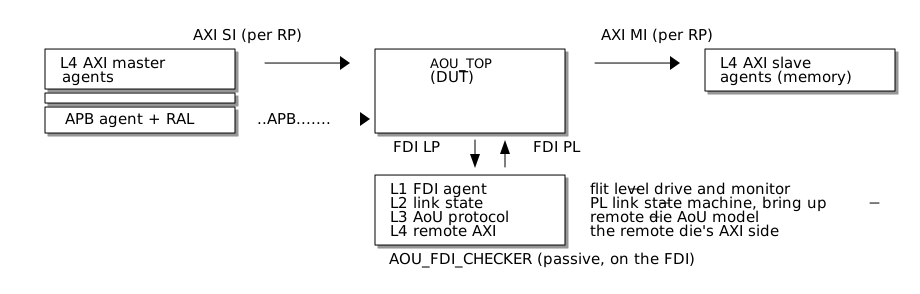
The remote die is modelled in four layers: L1 plays the Flit-Die Interface, L2 the PL link-state machine and bring-up, L3 the AoU protocol (message packing, credits, ordering), and L4 the AXI traffic on the remote side. AXI traffic entering a local RP is checked end to end against what the L4 remote model receives, and in the reverse direction. A passive AOU_FDI_CHECKER watches the FDI in both directions; its rules, and those of the AXI, APB and register checkers, are listed with their IDs in uvm/env/checkers/rules.csv.
The DUT parameters of a build are selected by CONFIG (1x512-sp64 by default: one RP at 512 bits, a 64-byte single-PHY FDI). The other configurations cover one to four RPs, mixed RP widths of 256/512/1024 bits, 32/64/128-byte FDI, two-PHY FDI and the non-default RX FIFO depths; make configs prints the table.
Components
| Component | Location | Description |
|---|---|---|
AOU_TOP |
tb/tb_top.sv |
The DUT of the T1 bench, with the RP count, RP data widths and FDI_CONFIG of the selected CONFIG. |
AXI agents (L4) |
uvm/env/axi/ |
AXI4 masters on the DUT’s slave ports, memory-backed AXI4 slaves on its master ports, and the remote die’s AXI side behind the L3 model; the protocol monitors and scoreboards check each transaction end to end. |
FDI agent (L1) and link-state agent (L2) |
uvm/env/fdi/l1/, uvm/env/fdi/l2/ |
Drive and monitor the Flit-Die Interface; play the PL link-state machine and bring-up, link events and low-power entry. |
AoU protocol model (L3) |
uvm/env/l3/ |
The remote die’s AoU protocol: message packing and unpacking, credits, ordering. |
APB agent and register model |
uvm/env/apb/, uvm/env/gen/aou_core_csr_uvm_pkg.sv |
Drives the APB port, activates the AOU, and reads and writes CSRs through the register model generated from csr/aou-core.rdl (IP Integration Collateral). |
AOU_FDI_CHECKER and checkers |
uvm/env/checker/, uvm/env/chk/, uvm/env/perf/ |
Passive FDI protocol checker; the AXI, APB, register and performance checkers. |
Register bench |
tb/aou_reg_top.sv (TB=reg) |
AOU_CORE_TOP with only its APB port driven; reset-value, bit-bash, access, reserved-field and alias tests against the register model. |
L3 unit bench, AXI self-test |
tb/aou_l3_unit_top.sv (TB=l3_unit), tb/aou_axi_selftest_top.sv (TB=axi_selftest) |
The L3 model and the FDI checker against each other without a DUT; the AXI agents in loopback. |
Testlists and grader |
testlists/, scripts/run_list.py, scripts/check_run.py, expected_fail.yaml |
TOML testlists (scenarios, seeds, groups such as smoke and functional); every run is graded, and failures caused by known DUT bugs are accepted as XFAIL when tied to the bug’s GitHub issue. |
Running the Testbench
From the bench directory, fetch the pinned dependencies once and then build and run:
cd hw/ip/aou/dv
make setup                                   # uvm-core, OCAH library, z3, PeakRDL, pywellen into .deps/
make test                                    # build TB=t1 CONFIG=1x512-sp64, run aou_sanity_test
make build SIM=verilator                     # or SIM=vcs (default when vcs is on PATH)
make run TEST=aou_dp_random_test SEED=3 PLUSARGS='+dp_dir=both'
make run TEST=aou_sanity_test WAVES=1        # waves into the run directory (FSDB/FST)
make build TB=reg && make run TB=reg TEST=aou_reg_access_test
python3 scripts/run_list.py --items smoke    # the bring-up gate (4 scenarios)
python3 scripts/run_list.py --items functional -j 16 --rid nightly
make check-config                            # sim configs, testlists, rules, RAL and docs freshness
make lint                                    # check-config, then Verible and Verilator lint
Each run ends with a verdict (PASS, XFAIL or FAIL) written to its run directory under out/; run_list.py collects them into results.csv and exits non-zero unless every run is PASS or XFAIL. Builds and runs go through LSF when bsub is available (LSF=0 runs on the current host). CI runs make check-config, builds the T1 and register benches on Verilator and runs the T1 bench’s ci group (smoke, the short lists and the datapath area) and the register bench’s smoke.
IP Integration Collateral
Machine-readable integration collateral is generated from the SystemRDL register source (csr/aou-core.rdl) using PeakRDL. This section describes the available outputs, the single-source workflow, and regeneration instructions.
Generated Outputs (Phase 1)
| Output | Path | Audience |
|---|---|---|
IP-XACT register map (IEEE 1685-2014) |
INTEG/ipxact/gen/aou_core_regmap.xml |
SoC integration tools (register only — memoryMaps element) |
C header |
DOC/csr/aou_core_csr.h |
Firmware / driver developers (#define macros for offsets and field masks) |
Interactive HTML docs |
DOC/csr/html/ |
Browsable register reference (any team) |
UVM register model |
INTEG/uvm/aou_core_csr_uvm_pkg.sv |
Verification (UVM uvm_reg_block package) — drop into your UVM env's RAL tier. |
Markdown register docs |
DOC/csr/aou-core-csrs.md |
Quick reference (also linked from Register Map) |
Note: the in-repo UVM testbench generates its own copy of the same model with the same PeakRDL command (hw/ip/aou/dv/scripts/regen_ral.sh, make ral) and commits it as hw/ip/aou/dv/uvm/env/gen/aou_core_csr_uvm_pkg.sv, so a make lint there fails when the RDL and the committed model drift apart. The INTEG/uvm/ package is the collateral for integrators' own UVM environments.
Single Source of Truth
All register information lives in the SystemRDL source file csr/aou-core.rdl. Every output listed above is derived from this single file — there is no separate register spreadsheet or hand-maintained IP-XACT register map.

To modify register definitions (addresses, field widths, access types, reset values, descriptions), edit csr/aou-core.rdl and regenerate. IMPORTANT: RTL is not generated from RDL so any modification to RDL files will not be reflected in the design.
Regeneration
From the repository root, activate the Python virtual environment and run the generation script:
source venv/bin/activate
bash scripts/gen_collateral.sh
The generation script automatically validates the IP-XACT output against the official Accellera IEEE 1685-2014 XSD schema after generation. The schema files are fetched from accellera.org on first run and cached locally (in INTEG/ipxact/schema/, gitignored).
To validate IP-XACT files independently:
python3 scripts/validate_ipxact.py INTEG/ipxact/gen/aou_core_regmap.xmlSee DOC/csr/README.md for a description of each output file and the top-level README.md for virtual-environment setup.
Planned: Full IP-XACT Component (Phase 2)
The Phase 1 IP-XACT output contains the <memoryMaps> element only (registers, fields, access types, reset values). A full IP-XACT component — including <busInterfaces> (ARM AMBA AXI4 and APB3), <ports>, and <model> parameters — is planned for a later phase.
This is deferred because AOU_CORE_TOP.sv uses SystemVerilog 2D packed arrays for its per-RP AXI ports (e.g., [RP_COUNT-1:0][AXI_ID_WD-1:0]), which have no clean single-dimension representation in IP-XACT. Once a wrapper module (AOU_CORE_TOP_WRAP) is created that flattens these into individual per-RP port signals, the full IP-XACT component will be generated by merging the PeakRDL register map into a hand-authored component template via scripts/merge_ipxact.py.
Timing Constraints (SDC)
Constraint files are located in INTEG/constraints/.
| File | Purpose |
|---|---|
aou_core_top.sdc |
Clock definitions, I/O delays, CDC, false paths |
aou_core_top.upf |
Power domain and supply network |
The SDC file defines timing constraints for synthesis and STA. All delay budget variables are declared at the top of the file and can be overridden by the integrating project. The port groups follow the current port list: INT_EARLY_WDT_ERR and INT_FDI_LINK_DOWN are in the combinational interrupt-output group, and the former I_*_BUS_CLEANY_COMPLETE inputs are gone.
Clock Definitions
| Clock | Port | Frequency | Period |
|---|---|---|---|
clk_core |
I_CLK |
1 GHz |
1.000 ns |
clk_apb |
I_PCLK |
100 MHz |
10.000 ns |
Both resets (I_RESETN, I_PRESETN) are constrained with set_false_path and should be synchronised externally or by the integrating design. The DFT scan-mode pin (TIEL_DFT_MODESCAN) is held at 0 via set_case_analysis in functional mode.
I/O Delay Budgeting Strategy
Two budgeting categories are used, based on whether the path between the I/O port and the nearest internal flop is combinational or registered:
| Path type | Internal budget | External budget | Rationale |
|---|---|---|---|
Combinational |
50% of clock period |
50% of clock period |
Mux/decode logic inside RTL takes some portion of cycle |
Registered |
30% of clock period |
70% of clock period |
Short wire path to first flop; external block gets more margin |
Interface classification summary:
-
APB Slave: Registered (via ASYNC_APB_BRIDGE 2-flop synchroniser on both sides). Constrained to clk_apb.
-
AXI Slave inputs (address, data, handshake to FIFOs): Registered — input data is captured directly into FIFO register arrays.
-
AXI Slave outputs (READY signals, read/bresp data): Combinational — passes through arbitration muxes.
-
AXI Master outputs (AR/AW/W channels): Combinational — data passes through FIFO read mux, arbitration mux (AXI4MUX_3X1), and REV_RS mux.
-
AXI Master inputs (R/B data, READY feedback): Combinational — feeds control logic and FIFO write.
-
FDI TX outputs (DATA, VALID, IRDY): Combinational. STALLACK outputs are registered. With TX_NXT_PACKING_EN = 1 the DATA output is driven from a register in AOU_TX_CORE through the FDI output mux only.
-
FDI RX inputs: Combinational — data/valid pass through an input mux. FLIT_CANCEL drives both sequential and combinational logic.
-
Interrupt/control signals: Combinational.
Clock Domain Crossings
The only CDC in AOU_CORE_TOP is between clk_core and clk_apb, handled by the ASYNC_APB_BRIDGE module which uses AOU_SOC_SYNCHSR (2-flop) synchronisers. The SDC uses set_clock_groups -asynchronous to exclude cross-domain paths from STA.
UPF Power Intent
The current UPF defines a single always-on power domain (PD_AOU_TOP) covering the integration scope (the AOU_TOP instance, which includes AOU_CORE_TOP and AOU_FDI_BRINGUP_CTRL, when integrating via AOU_TOP; or the AOU_CORE_TOP instance when integrating via AOU_CORE_TOP directly) with a VDD/VSS supply pair. No isolation, retention, or level-shifting strategies are required at this time. When power domains are introduced in the future, the UPF should be extended with create_power_domain for each switchable domain, along with appropriate isolation and retention strategies.
Library Cell Replacement
The RTL/LIB/ directory contains three behavioral reference models that are used by the design for reset infrastructure and clock-domain crossing. These models are functionally correct for simulation but must be replaced with process-appropriate implementations before synthesis or tapeout.
| Module | File | Parameters | Ports | Behavioral function | Where instantiated |
|---|---|---|---|---|---|
AOU_SOC_SYNCHSR |
RTL/LIB/AOU_SOC_SYNCHSR.v |
DW (width), RST_VAL (reset value), DEPTH (2/3/4) |
I_CLK, I_RESETN, I_D[DW-1:0] → O_Q[DW-1:0] |
Multi-stage synchroniser: per-bit shift register of depth DEPTH with async active-low reset to RST_VAL |
ASYNC_APB_BRIDGE_SI, ASYNC_APB_BRIDGE_MI (CDC synchronisation) |
AOU_SOC_GFMUX_LVT |
RTL/LIB/AOU_SOC_GFMUX_LVT.v |
DW (width) |
I_SEL, I_A[DW-1:0], I_B[DW-1:0] → O_Y[DW-1:0] |
Glitch-free 2:1 mux (I_SEL=0 selects I_A, I_SEL=1 selects I_B) |
AOU_CORE_TOP as u_sw_reset_mux (SW reset selection) |
AOU_SOC_BUF |
RTL/LIB/AOU_SOC_BUF.v |
DW (width) |
I_A[DW-1:0] → O_Y[DW-1:0] |
Non-inverting buffer (identity: O_Y = I_A) |
AOU_CORE_TOP as dft_persistent_buf_scan_resetn_sw (DFT persistent buffer on scan reset) |
Replacement approaches:
-
Drop-in replacement — Create new module definitions with the same module names and identical port/parameter interfaces, backed by standard cells or hard macros from the target process library. Replace the corresponding files in the filelist (RTL/LIB/filelist.f) with the new implementations.
-
In-place wrapper — Edit the provided module shells directly, replacing the behavioral assign/always bodies with instantiations of target-library primitives while keeping the module name and port interface unchanged.
Important considerations:
-
AOU_SOC_SYNCHSR is on the CDC path and must be replaced with a foundry-qualified synchroniser cell (or equivalent hardened multi-flop structure) to meet metastability MTBF requirements. The DEPTH parameter must be honoured.
-
AOU_SOC_GFMUX_LVT is on the reset mux path and must be replaced with a glitch-free clock/reset mux cell to avoid glitches during reset switching.
-
AOU_SOC_BUF is on the DFT scan-reset path. Replace with a buffer cell that will be preserved through synthesis optimisation (typically via a dont_touch or equivalent attribute).
-
The behavioral models can serve as a golden reference for verifying functional equivalence of the replacements.
Scan-Friendly Cell Requirements
Beyond functional correctness, each replacement cell must be compatible with ATPG scan insertion and pattern generation. The behavioral models have no scan awareness; the replacements must address this.
AOU_SOC_SYNCHSR — Scan-safe synchronizer
Standard multi-flop synchronizers cause X-propagation during scan shift because the asynchronous input crossing from the other clock domain is not controllable by the ATPG tool. The replacement synchronizer must be scan-safe via one of the following approaches:
-
Built-in scan bypass mux (preferred): The synchronizer cell includes a scan-mode mux that bypasses the asynchronous first-stage flop during shift. The ATPG tool holds the bypass active during shift and restores normal operation for capture. This is the standard approach used by foundry-provided synchronizer cells (e.g., SDFF-based sync cells with a scan-enable input).
-
ATPG tool constraint: If the replacement cell does not have a built-in bypass, the integrator must declare it as a synchronizer in the ATPG tool so the tool forces the input to a known value during shift (e.g., Synopsys set_dft_signal -type constant on the synchronizer input).
Foundry-provided synchronizer cells are strongly preferred because they are pre-characterized for both metastability MTBF and scan testability.
AOU_SOC_GFMUX_LVT — Clock/reset mux recognition
This cell sits on the scan-mode reset mux path (see TIEL_DFT_MODESCAN Usage). The replacement must be recognized by the ATPG tool as a clock or reset mux cell, not a generic data mux. If the tool treats it as a regular mux, it may toggle I_SEL during scan patterns, causing reset glitches that corrupt shift-register state and invalidate test patterns.
The integrator should:
-
Use a process library cell explicitly categorized as a clock/reset mux (e.g., a cell from the library's ICG or clock-mux family).
-
Apply the appropriate DFT tool attribute to prevent I_SEL toggling during scan. For example, in Synopsys DFT Compiler: set_dft_signal -view existing_dft -type ScanMux -port u_sw_reset_mux/I_SEL.
-
Verify in the ATPG tool's DFT rule check that the mux select is classified as a test-mode signal, not a scannable data input.
AOU_SOC_BUF — Optimization protection
This buffer drives the tied-low scan-reset bypass value into u_sw_reset_mux. Without protection, the synthesis tool will optimize it away (replacing it with a direct tie-off), which may cause the downstream reset mux to be optimized or restructured in ways that break the intended DFT architecture.
The replacement buffer must carry a dont_touch or size_only attribute (the specific attribute name depends on the synthesis tool) to ensure it survives all optimization passes, including:
-
Logic optimization and constant propagation
-
Incremental optimization during place-and-route
-
Post-route optimization