SMU Composition and Internal Wiring
The System Management Unit (SMU) combines the SMC, DTP, and optionally the SEP into a unified subsystem. The interface descriptions in the preceding sections apply directly when integrating the SMU, since the SMU inherits all three subsystems' ports. This section covers the module variants available to adopters, how the SMU wires its subsystems together internally, and what additional configuration it exposes.
1. Module Variants and IP Integration
OCAH core modules (smc.sv, sep.sv, dtp.sv, and the composite smu.sv)
expose logic-level interfaces only. All technology-specific components — PLLs,
PVT sensors, eFuse shims, memory macros, GPIO padrings, SPI controllers, and
external TRNG — are instantiated outside the core modules by the adopter. This
separation keeps the OCAH deliverable technology-neutral.
The figure below shows that boundary. smu exposes a technology integration
interface for each of these components, and a reference integration module
holds the shims, models and macros behind them. An adopter keeps the interfaces
and replaces what lies below the boundary with its own technology IP.
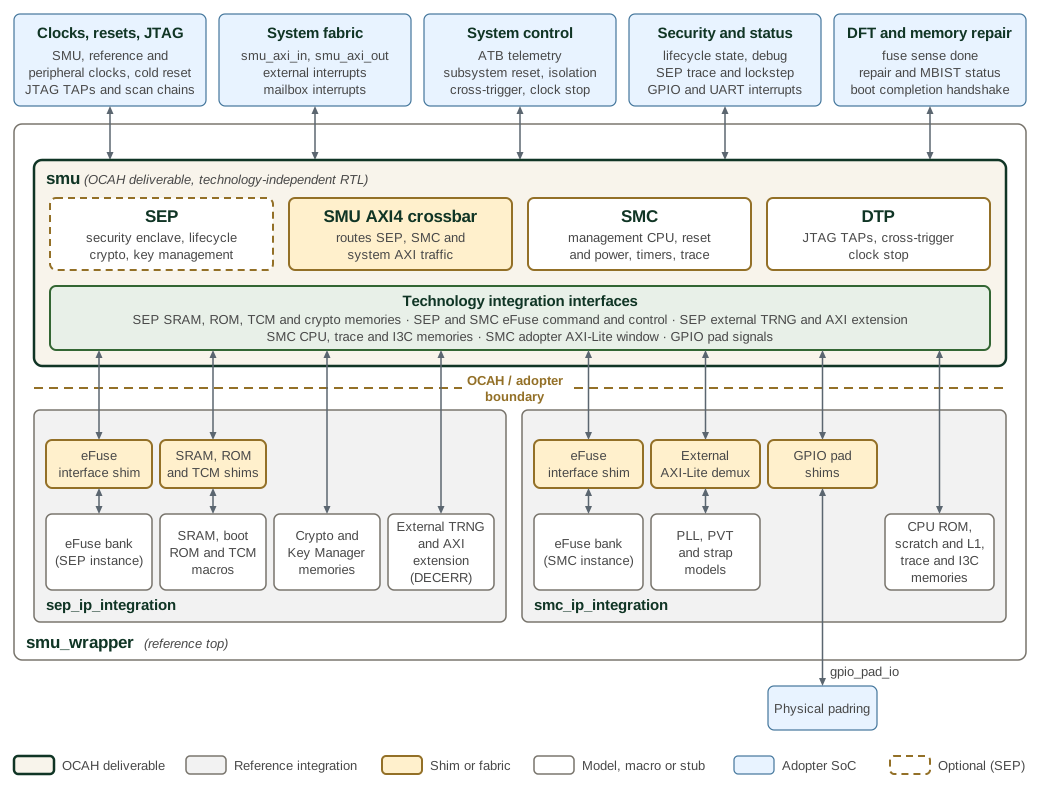
The repository provides reference wrappers that demonstrate how to bridge the gap between OCAH core interfaces and adopter-specific IP:
-
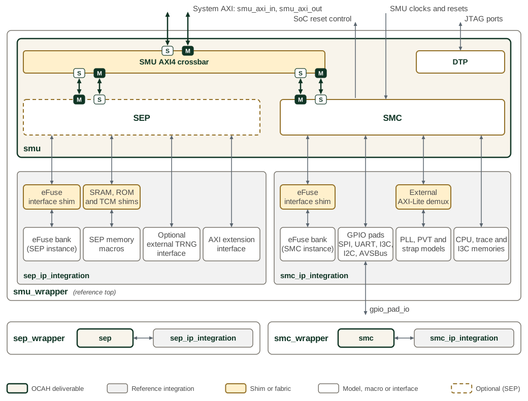
smu_wrapper.svwrapssmu.svwith pad-level signal handling for clocks, resets, GPIO, eFuse, and JTAG interfaces. It internally instantiatessmc_ip_integration.svfor SMC-related vendor IP andsep_ip_integration.svfor SEP-related vendor IP. Each integration module holds its own eFuse interface shim and eFuse bank. -
smc_wrapper.svprovides an equivalent reference wrappingsmc.svalone, useful when integrating the SMC without the DTP/SEP subsystems.
Neither the wrappers nor the IP integration modules are part of the OCAH deliverable; they exist as integration guides. Adopters must develop their own equivalents following the interface patterns demonstrated in these modules. The interface contracts at the module boundaries ensure technology substitution without modifying the verified OCAH logic.
The figure below illustrates the relationship between the OCAH core modules, the wrapper layer, and the IP integration modules.
1.1. IP Integration Modules
smc_ip_integration.sv demonstrates integration of SMC-side technology
components: PLL wrappers (generating pll_cgm_clk_o and pll_awm_clk_o),
PVT sensor interfaces, eFuse shims, GPIO padring logic, memory macros (ROM,
scratchpad RAM, cache tag and data arrays), and trace memory instances.
sep_ip_integration.sv demonstrates integration of SEP-side technology
components: SEP memory macros (TCM, scratch SRAM, boot ROM, OTBN IMEM/DMEM,
Key Manager ROM/SRAM), eFuse shim, external TRNG, and SPI controller selection.
1.2. Wrapper Clock Architecture
The behavioral pll_wrap model is a DV/reference
placeholder: it free-runs refclk, sys_clk, and periph_clk at 100 / 800 / 200 MHz
(+pll_sys_period_ns=10 runs sys_clk at 100 MHz; with +pll_osc_bench a bench
toggles the oscillator nets itself), muxes sys and periph with ref
through prim_clock_mux2 then prim_ag_clk_mux, and terminates the AXI-Lite PLL
control interface with OKAY. It is not a synthesis stand-in. An adopter who
replaces smc_ip_integration supplies equivalent clocks internally; the
bare cores still have the three clock inputs.
2. Clock and Reset Architecture
Connect clk_smu_i to the primary system clock and clk_ref_i to a stable
reference source. The DTP operates on TCK for JTAG logic and on the system clock
for cross-trigger and AXI bridges. Reset sequencing follows the SMC flow; the
DTP JTAG state machine uses pwr_on_rst_ni, which the SMU connects to the SMC
powergood_stable_o output. The SMU internally connects DTP debug paths to the
SMC and optionally instantiates the SEP when CFG.SEP is set to 1. The full
interconnection details are described in SMC-DTP Internal Interconnection and
SEP-Conditional Wiring below.
3. SMU AXI Crossbar Address Map
Inside the SMU, the smu_axi_xbar module routes traffic between three
AXI4 manager/subordinate pairs: the SEP outbound master (sep_out),
the SMC outbound master (smc_out), and the external SMU AXI input
(ext_in / smu_axi_in). The corresponding targets are the SEP and
SMC inbound subordinates, and the external SMU AXI output
(ext_out / smu_axi_out).
The SMU instantiates smu_axi_xbar only when CFG.SEP is 1. When CFG.SEP
is 0, AXI ID-width converters connect the SMC system AXI ports to
smu_axi_in / smu_axi_out instead: every SMC-initiated transaction leaves
through smu_axi_out, every smu_axi_in transaction targets the SMC, and the
aperture rules below do not apply. The smu_axi_in / smu_axi_out port types
are the same in both configurations.
Connectivity is described in SMU AXI Crossbar; the split between hardware-fixed behavior and firmware-programmable apertures is documented in OCAH Memory Map.
The crossbar uses a runtime address map with two rules, the SEP and
SMC apertures, both programmable at runtime. ext_out has no address
rule. The apertures are driven as follows:
-
sep_global_base_addr_i/sep_region_size_icome from thesep_cpu_ctrlCSRsSEP_GLOBAL_BASE_ADDR/SEP_REGION_SIZE, exposed at thesep.svboundary assep_global_base_addr_o/sep_region_size_o, and at thesmu.svboundary assep_global_base_o/sep_region_size_o(both 56-bit).SEP_REGION_SIZEis a 32-bit CSR field, zero-extended to 56-bit at the SEP system CSR; the xbar input takes only the lower 32 bits.SEP_REGION_SIZEdefines the SEP global/chiplet aperture for SMU routing and SEP inbound global-to-local remap. It is distinct from the SEP CPU’s architectural local-alias span.SEP_REGION_SIZEcurrently resets to0x0100_0000(16 MiB). Tied to'0at thesmu.svboundary whenCFG.SEPis0. -
smc_global_base_addr_i/smc_region_size_icome from thesmc_base_configCSRsGLOBAL_BASE/REGION_SIZE, exposed at both thesmc.svandsmu.svboundaries assmc_global_base_o(56-bit) /smc_region_size_o(32-bit).REGION_SIZEresets to0x0100_0000(16 MiB).
SEP, SMC, and smu_axi_xbar all run on clk_smu_i, so these
quasi-static CSR fields need no clock-domain crossing. The crossbar’s
address arithmetic is done on 57-bit widened sums. For where unmatched
requests go, and which requests return DECERR, see
SMU AXI crossbar routing.
3.1. Firmware programming order
Firmware must program SEP_GLOBAL_BASE_ADDR / SEP_REGION_SIZE and
SMC GLOBAL_BASE / REGION_SIZE during early boot, before any
cross-subsystem AXI traffic is issued, and must ensure the two
apertures do not overlap and both fall within the chiplet-visible SMU
envelope assigned by the integrator. The SMU crossbar does not itself
constrain envelope size.
See OCAH Memory Map for the responsibility split between integrator, firmware, and the internal SEP/SMC address maps.
4. SMU Default Parameters
The DTP JTAG features, identification, cross trigger, and pipeline depths are
fields of the CFG parameter, of type smu_pkg::smu_cfg_t. CFG defaults to
the smu_pkg::SmuConfigs preset that the CFG_IDX parameter selects:
smu_pkg::DefaultCfg at the default index 0, or smu_pkg::NoSepCfg, which
differs only in SEP, at index 1. A CFG passed directly takes precedence over
CFG_IDX. Flows that override parameters with elaborate -param, which cannot
set a struct, select the preset through CFG_IDX.
The parameters of smu are listed in smu.
SEP-related DTP configuration has no smu_cfg_t field of its own.
The SMU derives SEP debug/STAP enablement from CFG.SEP and
wires the corresponding DTP interfaces internally to the SEP block when CFG.SEP=1.
5. IC_RESET TDR Structure
The DTP primary TAP implements the IEEE 1149.1-2013 §17 IC_RESET TDR as three
independently enabled slices plus a single reset_hold bit nearest TDO. At the
SMU the scan order from TDI to TDO is:
TDI → SMC slice → SEP slice → external slice → reset_hold → TDOThe SMU enables the SMC slice unconditionally, the SEP slice when CFG.SEP=1
(otherwise that slice has width 0 and is omitted), and the external slice when
JTAG_IC_RESET_ENABLE is set. Each slice is a packed struct with .ovrd and
.val halves of equal width; jtag_ptap sizes the slice from $bits(type)/2.
Each port has the reset-enable and reset-control pair IEEE §17 requires, with
reset_enable nearer TDO. .val carries reset_control, and .ovrd carries
the inverse of reset_enable. Declaration order within each half is the TDI-to-TDO
scan order: the first field is nearest TDI.
| Slice | Ports | Defined by | Consumed by |
|---|---|---|---|
SMC |
68 |
OCAH ( |
SMC reset unit; SMU-internal, no SMU port |
SEP |
8 when |
OCAH ( |
SEP reset controller; SMU-internal, no SMU port |
External |
|
Adopter ( |
SMU output |
|
1 bit |
IEEE 1149.1 §17 |
Nearest TDO; not a reset port |
The TDR length is 2 * (SMC ports + SEP ports + external ports) + 1. Programming
order and reset_enable polarity are in the DTP JTAG chapter of the Technical
Reference Manual.
5.1. SMC slice (TDI to TDO)
The SMC slice covers the SMC reset domains and the 32 managed-subsystem (SS)
cold and warm resets. Vector index [31] of each SS field is nearer TDI than
[0].
| Port | Reset domain |
|---|---|
|
Per-subsystem warm reset |
|
Per-subsystem cold reset |
|
SMC cold reset |
|
SMC cool reset |
|
SMC warm reset |
|
Fuse reset (nearest the SEP slice) |
5.2. SEP slice (TDI to TDO)
When CFG.SEP=1 the SEP slice covers the SEP main reset and the crypto, Key
Manager, and TRNG resets consumed by sep_reset_ctrl. abr_jtag_rst_n is
nearest TDI.
| Port | Reset domain |
|---|---|
|
Adams Bridge |
|
TRNG |
|
SEP main reset |
|
KMAC |
|
HMAC |
|
AES |
|
OTBN |
|
Key Manager (nearest the external slice) |
5.3. External slice (adopter-defined)
The external slice is reserved for reset overrides on logic instantiated
outside the SMU. OCAH does not name its ports. Set the SMU type parameter
ic_reset_ext_t to a packed struct with .ovrd and .val halves of equal
width, and route jtag_ic_reset_ext_o to that logic. The parameter default
(jtag_tap_pkg::jtag_ic_reset_default_t) is a single-override stub. Clear
JTAG_IC_RESET_ENABLE when no external overrides are required.
Declare a new external override at each half’s MSB so already-assigned TDR positions do not shift. Extra subsystem reset controls beyond the SMC slice use this typed port.
6. DTP Parameter Pass-Through
The SMU passes through most DTP parameters to allow integrator customization. Type parameters are set internally based on SMC package types.
6.1. JTAG Configuration Parameters
| Parameter | SMU Default | Pass-through | Notes |
|---|---|---|---|
|
1 |
Yes |
Boundary scan enabled |
|
1 |
Yes |
|
|
1 |
Yes |
|
|
1 |
Yes |
|
|
1 |
Yes |
|
|
1 |
Yes |
|
|
1 |
Yes |
|
|
1 |
Yes |
|
|
1 |
No |
SMU routes this to the DTP’s |
|
1 |
Yes |
|
|
1 ( |
No |
Derived internally from |
|
1 |
Yes |
|
|
1 |
Yes |
Port array size equals parameter value; when set to 0, array size is 1 (tie-off required) |
6.2. JTAG ID Parameters
| Parameter | SMU Default | Pass-through | Notes |
|---|---|---|---|
|
|
Yes |
Manufacturer ID |
|
|
Yes |
Part number |
|
|
Yes |
Silicon revision |
|
|
Yes |
DTP IP major version |
6.3. Cross Trigger Parameters
| Parameter | SMU Default | DTP Internal | Pass-through | Notes |
|---|---|---|---|---|
|
16 |
CFG |
Yes |
External CTP count |
|
8 |
CFG + |
Yes |
SMU-exposed count; DTP adds the SMC-reserved lanes |
|
8 |
CFG + |
Yes |
SMU-exposed count; DTP adds the SMC-reserved lane |
|
32 bits, low 8 consumed |
DTP width |
Yes |
SMC-reserved DTP mode bits are 0 (pulse-sync) |
The SMU remaps DTP internal-CT lanes above the SMC reservation onto the SMU-exposed ports. Clock-stop request lane 0 is reserved for SMC; the SMU exposes the remaining DTP lanes.
6.4. Pipeline Depth Parameters
| Parameter | SMU Default | Pass-through | Notes |
|---|---|---|---|
|
|
Yes |
SMC OTP read pipeline depth |
|
|
Yes |
SMC OTP write pipeline depth |
|
|
No |
Fixed to |
|
|
No |
Fixed to |
|
|
Yes |
SMC fabric read pipeline depth |
|
|
Yes |
SMC fabric write pipeline depth |
6.5. Type Parameters
The following type parameters are set internally by the SMU and are not exposed for integrator configuration.
| Parameter | Set To | Notes |
|---|---|---|
|
|
JTAG TAP control struct |
|
|
JTAG scan control struct |
|
|
SMC debug AXI request |
|
|
SMC debug AXI response |
|
|
SMC IC_RESET TDR slice |
|
|
SEP IC_RESET TDR slice |
|
|
SMC OTP AXI-Lite request |
|
|
SMC OTP AXI-Lite response |
|
|
SEP OTP AXI-Lite request (error slave when |
|
|
SEP OTP AXI-Lite response (error slave when |
|
|
Cross trigger CSR request |
|
|
Cross trigger CSR response |
7. DTP Port Mapping
The following tables define the complete DTP port list as connected within the SMU. Ports marked "SMU external port" are exposed on the SMU boundary for integrator connection. Ports marked with a subsystem name (e.g. SMC, SEP) are wired internally within the SMU.
7.1. Clock and Reset
| Port | Direction | Width | SMU Connection |
|---|---|---|---|
|
input |
1 |
SMU |
|
input |
1 |
SMC |
|
input |
1 |
SMC |
7.2. Primary JTAG TAP Interface
| Port | Direction | Width | SMU Connection |
|---|---|---|---|
|
input |
|
SMU external port |
|
input |
1 |
SMU external port |
|
output |
1 |
SMU external port |
|
output |
1 |
SMU external port |
7.3. Boundary Scan Interface
| Port | Direction | Width | SMU Connection |
|---|---|---|---|
|
output |
|
SMU external port |
|
input |
1 |
SMU external port |
|
output |
1 |
SMU external port |
7.4. I/O STAP Interface
| Port | Direction | Width | SMU Connection |
|---|---|---|---|
|
output |
|
SMU external port |
|
input |
1 |
SMU external port |
|
output |
1 |
SMU external port |
|
output |
1 |
SMU external port |
7.5. SMC Debug STAP Interface
| Port | Direction | Width | SMU Connection |
|---|---|---|---|
|
output |
|
SMC |
|
input |
1 |
SMC |
|
output |
1 |
SMC |
|
output |
1 |
Internal only; not consumed by SMC |
7.6. SEP Debug STAP Interface
| Port | Direction | Width | SMU Connection |
|---|---|---|---|
|
output |
|
SEP |
|
input |
1 |
SEP |
|
output |
1 |
SEP |
|
output |
1 |
Internal only; not consumed by SEP at SMU level |
7.7. Extra STAP Interfaces
| Port | Direction | Width | SMU Connection |
|---|---|---|---|
|
output |
|
SMU external port |
|
input |
[JtagNumExtraStapPorts-1:0] |
SMU external port |
|
output |
[JtagNumExtraStapPorts-1:0] |
SMU external port |
|
output |
[JtagNumExtraStapPorts-1:0] |
SMU external port |
7.8. Extended STAP Scan Interface
| Port | Direction | Width | SMU Connection |
|---|---|---|---|
|
output |
|
SMU external port |
|
input |
1 |
SMU external port |
|
output |
1 |
SMU external port |
7.9. DFD iJTAG Interface
| Port | Direction | Width | SMU Connection |
|---|---|---|---|
|
output |
|
SMU external port |
|
input |
1 |
SMU external port |
|
output |
1 |
SMU external port |
7.10. DFT iJTAG Interfaces
| Port | Direction | Width | SMU Connection |
|---|---|---|---|
|
output |
|
Secure DFT iJTAG SMU external port |
|
input |
1 |
Secure DFT iJTAG SMU external port |
|
output |
1 |
Secure DFT iJTAG SMU external port |
|
output |
|
Non-secure DFT iJTAG SMU external port |
|
input |
1 |
Non-secure DFT iJTAG SMU external port |
|
output |
1 |
Non-secure DFT iJTAG SMU external port |
7.11. SMC Fabric Debug AXI Interface
| Port | Direction | Width | SMU Connection |
|---|---|---|---|
|
output |
|
SMC |
|
input |
|
SMC |
7.12. SMC OTP Debug AXI-Lite Interface
| Port | Direction | Width | SMU Connection |
|---|---|---|---|
|
output |
|
SMC |
|
input |
|
SMC |
7.13. SEP OTP Debug AXI-Lite Interface
When CFG.SEP=1, this interface connects to the SEP axil_sep_otp_jtag_* ports.
When CFG.SEP=0, the SMU instantiates u_sep_otp_axil_err_slv, which responds
with DECERR to all transactions.
| Port | Direction | Width | SMU Connection |
|---|---|---|---|
|
output |
|
SEP |
|
input |
|
SEP |
7.14. Clock Control
| Port | Direction | Width | SMU Connection |
|---|---|---|---|
|
output |
1 |
SMU external port: |
7.15. Boot Stall Control
| Port | Direction | Width | SMU Connection |
|---|---|---|---|
|
output |
1 |
SMC |
|
output |
1 |
SMC |
7.16. JTAG Reset Control
| Port | Direction | Width | SMU Connection |
|---|---|---|---|
|
output |
|
SMC |
|
output |
|
SEP |
|
output |
|
SMU |
7.17. JTAG State Outputs
| Port | Direction | Width | SMU Connection |
|---|---|---|---|
|
output |
|
SMU external port |
|
output |
|
SMU external port |
7.18. Cross Trigger CSR AXI-Lite Interface
| Port | Direction | Width | SMU Connection |
|---|---|---|---|
|
input |
|
SMC |
|
output |
|
SMC |
7.19. Cross Trigger Matrix Interface
| Port | Direction | Width | SMU Connection |
|---|---|---|---|
|
output |
[XtrigNumIntCt-1:0] |
SMC-reserved DTP lanes stay inside the SMU; remaining lanes are the SMU external port |
|
input |
[XtrigNumIntCt-1:0] |
SMC-reserved DTP lanes tied off; remaining lanes are the SMU external port |
|
input |
[XtrigNumIntCt-1:0] |
SMC-reserved DTP lanes from SMC |
|
output |
[XtrigNumIntCt-1:0] |
SMC-reserved DTP lanes unused; remaining lanes are the SMU external port |
The low smu_pkg::XtrigSmcIntCtLanes DTP internal-CT lanes are reserved for
SMC (both bits of xtrigger_ss_o). The SMU exposes the remaining DTP lanes, so
the SMU XTRIG_NUM_INT_CT field is that many less than DTP’s. The SMC uses
pulse-synchronization mode, so ack signals for the reserved lanes are unused:
the DTP xtrig_ctm_src_ack_i reserved slice is tied to '0 and
xtrig_ctm_dst_ack_o reserved bits are left unconnected. The usage of ack
signals depends on the XTRIG_INT_CT_MODE parameter: when a mode bit is 0
(pulse synchronization), the corresponding ack is unused; when 1 (req/ack
handshaking), the ack must be connected to the cross trigger endpoint.
7.20. Clock Stop Request Interface
| Port | Direction | Width | SMU Connection |
|---|---|---|---|
|
input |
[XtrigNumClkStopReq-1:0] |
DTP lane 0: SMC |
Clock-stop request lane 0 is reserved for SMC. The SMU exposes the remaining
DTP lanes, so the SMU XTRIG_NUM_CLK_STOP_REQ field is
smu_pkg::XtrigSmcClkStopLanes less than DTP’s.
7.21. Cross Trigger Port GPIO Interface
CTP signals from DTP are ported through the SMU and are direct
smu_wrapper external ports (connected through the .* SMU instantiation).
The adopter must connect them to GPIO pad logic; no tie-off or dangling is
present in the wrapper itself. Widths follow CFG.XTRIG_NUM_CTP (default 16).
| Port | Direction | Width | SMU Connection |
|---|---|---|---|
|
output |
[XtrigNumCtp-1:0] |
SMU external port; connect to GPIO pad logic |
|
output |
[XtrigNumCtp-1:0] |
SMU external port; connect to GPIO pad logic |
|
input |
[XtrigNumCtp-1:0] |
SMU external port; connect to GPIO pad logic |
|
output |
[XtrigNumCtp-1:0] |
SMU external port; connect to GPIO pad logic |
|
output |
[XtrigNumCtp-1:0] |
SMU external port; connect to GPIO pad logic |
|
output |
[XtrigNumCtp-1:0] |
SMU external port; connect to GPIO pad logic |
|
input |
[XtrigNumCtp-1:0] |
SMU external port; connect to GPIO pad logic |
|
output |
[XtrigNumCtp-1:0] |
SMU external port; connect to GPIO pad logic |
8. SMC Port Mapping
The following tables define the complete SMC port list as connected within the SMU. Ports marked "SMU external port" are exposed on the SMU boundary. Ports marked with "DTP" or "SEP" are wired internally.
8.1. Clocks
| Port | Direction | Width | SMU Connection |
|---|---|---|---|
|
input |
1 |
SMU |
|
input |
1 |
SMU external port |
|
input |
1 |
SMU external port |
8.2. Resets
| Port | Direction | Width | SMU Connection |
|---|---|---|---|
|
input |
1 |
SMU external port |
|
output |
1 |
SMU external port |
|
output |
1 |
SMU external port + DTP |
8.3. System AXI Input
| Port | Direction | Width | SMU Connection |
|---|---|---|---|
|
input |
|
SMU external port |
|
output |
|
SMU external port |
8.4. JTAG AXI Input
| Port | Direction | Width | SMU Connection |
|---|---|---|---|
|
input |
|
DTP |
|
output |
|
DTP |
8.5. SMC OTP JTAG AXI-Lite
| Port | Direction | Width | SMU Connection |
|---|---|---|---|
|
input |
|
DTP |
|
output |
|
DTP |
8.6. SEP AXI Input
When CFG.SEP=0, the SEP AXI subordinate input is tied off to '0 and the
response output is left unconnected. When CFG.SEP=1, the SMU drives this path from
the SEP-to-SMC dedicated AXI connection.
| Port | Direction | Width | SMU Connection |
|---|---|---|---|
|
input |
|
Tied off to |
|
output |
|
Unconnected (no transactions to respond to) |
8.7. AXI Output
| Port | Direction | Width | SMU Connection |
|---|---|---|---|
|
output |
|
SMU external port |
|
input |
|
SMU external port |
8.8. DTP CSR Interface
| Port | Direction | Width | SMU Connection |
|---|---|---|---|
|
output |
|
DTP |
|
input |
|
DTP |
8.9. Adopter Peripheral Window AXI-Lite
| Port | Direction | Width | SMU Connection |
|---|---|---|---|
|
output |
|
SMU external port (to adopter peripherals) |
|
input |
|
SMU external port (from adopter peripherals) |
8.10. eFuse Interface
| Port | Direction | Width | SMU Connection |
|---|---|---|---|
|
output |
|
SMU external port |
|
input |
|
SMU external port |
|
output |
|
SMU external port |
|
input |
|
SMU external port |
|
output |
|
SMU external port |
8.11. GPIO Data Signals
| Port | Direction | Width | SMU Connection |
|---|---|---|---|
|
output |
[NumGpioWraps-1:0] |
SMU external port |
|
input |
[NumGpioWraps-1:0] |
SMU external port |
|
output |
[NumGpioWraps-1:0] |
SMU external port |
|
output |
[NumGpioWraps-1:0] |
SMU external port |
|
output |
[NumGpioWraps-1:0] |
SMU external port |
8.12. GPIO External Pins
| Port | Direction | Width | SMU Connection |
|---|---|---|---|
|
input |
1 |
SMU external port |
8.13. ATB Telemetry
| Port | Direction | Width | SMU Connection |
|---|---|---|---|
|
input |
1 |
SMU external port |
|
input |
1 |
SMU external port |
|
input |
|
SMU external port |
|
input |
|
SMU external port |
|
output |
[NumTelemetryReceivers-1:0] |
SMU external port |
|
input |
[NumTelemetryReceivers-1:0] |
SMU external port |
|
output |
[NumTelemetryReceivers-1:0] |
SMU external port |
|
input |
[NumTelemetryReceivers-1:0] |
SMU external port |
8.14. DED/WDT
| Port | Direction | Width | SMU Connection |
|---|---|---|---|
|
output |
1 |
SMU external port |
|
output |
1 |
SMU external port |
|
output |
1 |
SMU external port |
8.15. Region Size
| Port | Direction | Width | SMU Connection |
|---|---|---|---|
|
output |
[31:0] |
SMU external port |
8.16. External Interrupts
| Port | Direction | Width | SMU Connection |
|---|---|---|---|
|
input |
[NUM_EXT_INTERRUPTS-1:0] |
SMU external port |
|
input |
[7:0] |
Internal: from SEP |
|
input |
1 |
Internal: |
8.17. Fuse Signals
| Port | Direction | Width | SMU Connection |
|---|---|---|---|
|
output |
1 |
SMU external port |
|
output |
1 |
SMU external port |
8.18. DFT Signals
| Port | Direction | Width | SMU Connection |
|---|---|---|---|
|
output |
1 |
SMU external port |
|
input |
1 |
SMU external port |
|
output |
1 |
Internal: drives SEP |
8.19. Lifecycle State
| Port | Direction | Width | SMU Connection |
|---|---|---|---|
|
output |
[2*LcStateWidth-1:0] |
SEP lifecycle state when |
|
output |
1 |
Differential encoding error reported by the SEP (when |
8.20. Mailbox Interrupts
| Port | Direction | Width | SMU Connection |
|---|---|---|---|
|
output |
[NumMailboxes-1:0] |
SMU external port |
8.21. Reset Unit Signals
| Port | Direction | Width | SMU Connection |
|---|---|---|---|
|
input |
1 |
SMU external port |
|
output |
[31:0] |
SMU external port |
|
input |
[31:0] |
SMU external port |
|
output |
[31:0] |
SMU external port |
|
output |
|
SMU external port |
|
output |
1 |
SMU external port |
8.22. CPU Memory Signals
| Port | Direction | Width | SMU Connection |
|---|---|---|---|
|
output |
|
SMU external port |
|
input |
|
SMU external port |
|
output |
|
SMU external port |
|
input |
|
SMU external port |
|
output |
|
SMU external port |
|
input |
|
SMU external port |
|
output |
|
SMU external port |
|
input |
|
SMU external port |
|
output |
|
SMU external port |
|
input |
|
SMU external port |
|
output |
|
SMU external port |
|
input |
|
SMU external port |
8.23. Memory Init
| Port | Direction | Width | SMU Connection |
|---|---|---|---|
|
input |
1 |
SMU external port |
|
output |
1 |
SMU external port |
8.24. System Timer OCTS Interface
| Port | Direction | Width | SMU Connection |
|---|---|---|---|
|
output |
[63:0] |
SMU external port |
8.25. Reset Overrides (from DTP)
| Port | Direction | Width | SMU Connection |
|---|---|---|---|
|
input |
|
DTP |
8.26. DFD Signals
| Port | Direction | Width | SMU Connection |
|---|---|---|---|
|
output |
1 |
SMU external port |
|
input |
1 |
DTP |
|
output |
1 |
DTP |
8.27. Cross Trigger Interface
| Port | Direction | Width | SMU Connection |
|---|---|---|---|
|
input |
|
SMU internal: DTP |
|
output |
|
SMU internal: SMC → DTP |
8.28. Trace Memory
| Port | Direction | Width | SMU Connection |
|---|---|---|---|
|
output |
|
SMU external port |
|
input |
|
SMU external port |
8.29. External Debug Bus
| Port | Direction | Width | SMU Connection |
|---|---|---|---|
|
input |
[127:0] |
SMU external port |
8.30. Test Mode
| Port | Direction | Width | SMU Connection |
|---|---|---|---|
|
input |
1 |
SMU external port |
|
input |
1 |
SMU external port |
9. SMC-DTP Internal Interconnection
The following table summarizes the key internal connections between the DTP and SMC within the SMU. These connections are not visible on the SMU boundary.
| Connection | DTP Port | SMC Port | Direction | Notes |
|---|---|---|---|---|
AXI Debug Bus |
|
|
DTP → SMC |
|
|
|
SMC → DTP |
||
AXI OTP Bus |
|
|
DTP → SMC |
|
|
|
SMC → DTP |
||
DTP CSR Bus |
|
|
SMC → DTP |
|
|
|
DTP → SMC |
||
JTAG SMC Reset Overrides |
|
|
DTP → SMC |
Packed |
DTP Reset |
|
|
SMC → DTP |
|
Cross Trigger reserved lanes |
|
|
SMC → DTP |
|
Clock Stop reserved lane |
|
|
SMC → DTP |
|
Boot Stall |
|
|
DTP → SMC |
|
|
|
DTP → SMC |
10. SEP-Conditional Wiring
SEP-related interfaces are handled internally within the SMU. Their behavior
depends on CFG.SEP.
| Module/Signal | Implementation | Description |
|---|---|---|
SMU AXI fabric |
|
System-level AXI routing between SEP, SMC and the SMU boundary |
SMC SEP AXI Input |
|
Dedicated SEP-to-SMC subordinate path |
DTP SEP OTP JTAG |
SEP |
SEP OTP debug AXI-Lite path |
DTP SEP STAP return |
SEP |
SEP JTAG STAP return path |
SMU |
|
Internal SEP-to-SMC mailbox interrupts when |
SMC |
|
SEP watchdog reset input to SMC |
10.1. Other Internal Tie-offs
| Module | Port | Tie-off Value | Reason |
|---|---|---|---|
DTP |
|
|
SMC uses pulse-sync mode |
The remaining DTP xtrig_ctm_src_ack_i lanes (exposed as SMU
xtrig_ctm_src_ack_i[XTRIG_NUM_INT_CT-1:0]) are ported out through the SMU.
The integrator should tie off to '0 when using pulse-sync mode
(XTRIG_INT_CT_MODE bit = 0), or connect to actual ack signals when using
req/ack mode (bit = 1).
11. SMU Port Interface
The SMU exposes a single consolidated boundary that an adopter connects to
at the chip or chiplet level. The following table defines all SMU top-level
ports including clock, reset, JTAG, cross trigger, SMC-originated interfaces
(AXI, GPIO, eFuse, PLL, PVT, memory), and SEP passthrough interfaces
(memory macros, eFuse, crypto SRAM, SPI, AXI extension). Ports prefixed
with sep_ are only active when CFG.SEP=1.
The generated module and port pages are in the TRM under RTL Modules Reference. This table keeps each port’s connection and tie-off default.
| Interface Name | Type | Direction | Width | Description | Connection | Default value (if applicable) |
|---|---|---|---|---|---|---|
|
|
Input |
1 |
Primary SMU clock domain. Shared by SMC and DTP system logic. |
PLL output |
N/A |
|
|
Input |
1 |
Reference clock domain for timing-sensitive operations. |
PLL reference clock |
N/A |
|
|
Input |
1 |
Cold reset (active low). Assertion and deassertion are synchronous to |
System cold reset |
N/A |
|
|
Output |
1 |
Stable cold reset synchronized to reference clock domain (active low). |
Downstream subsystems |
N/A |
|
|
Input |
1 |
Power-good indication from supply supervisor. |
Power supply supervisor |
N/A |
|
|
Input |
- |
Primary JTAG TAP control (TCK, TMS, TRST_N). |
External JTAG pads |
N/A |
|
|
Input |
1 |
Primary JTAG TDI. |
External JTAG pads |
N/A |
|
|
Output |
1 |
Primary JTAG TDO. |
External JTAG pads |
N/A |
|
|
Output |
1 |
Primary JTAG TDO output enable. |
External JTAG pads |
N/A |
|
|
Output |
- |
Boundary scan control. |
Boundary scan chain |
N/A |
|
|
Input |
1 |
Boundary scan data in. |
Boundary scan chain |
N/A |
|
|
Output |
1 |
Boundary scan data out. |
Boundary scan chain |
N/A |
|
|
Output |
- |
I/O STAP TAP control. |
I/O STAP host |
N/A |
|
|
Input |
1 |
I/O STAP TDI. |
I/O STAP host |
Tie to '0 if unused |
|
|
Output |
1 |
I/O STAP TDO. |
I/O STAP host |
N/A |
|
|
Output |
1 |
I/O STAP TDO output enable. |
I/O STAP host |
N/A |
|
|
Output |
|
Extra STAP TAP control array. |
Extra STAP hosts |
Tie to '0 if unused |
|
|
Input |
|
Extra STAP TDI array. |
Extra STAP hosts |
Tie to '0 if unused |
|
|
Output |
|
Extra STAP TDO array. |
Extra STAP hosts |
N/A |
|
|
Output |
|
Extra STAP TDO output enable array. |
Extra STAP hosts |
N/A |
|
|
Output |
- |
Extended STAP scan control. |
STAP scan chain |
N/A |
|
|
Input |
1 |
Extended STAP scan data in. |
STAP scan chain |
N/A |
|
|
Output |
1 |
Extended STAP scan data out. |
STAP scan chain |
N/A |
|
|
Output |
- |
DFD iJTAG scan control. |
DFD iJTAG chain |
N/A |
|
|
Input |
1 |
DFD iJTAG scan data in. |
DFD iJTAG chain |
N/A |
|
|
Output |
1 |
DFD iJTAG scan data out. |
DFD iJTAG chain |
N/A |
|
|
Output |
- |
Secure DFT iJTAG scan control. |
Secure DFT iJTAG chain |
N/A |
|
|
Input |
1 |
Secure DFT iJTAG scan data in. |
Secure DFT iJTAG chain |
N/A |
|
|
Output |
1 |
Secure DFT iJTAG scan data out. |
Secure DFT iJTAG chain |
N/A |
|
|
Output |
- |
Non-secure DFT iJTAG scan control. |
Non-secure DFT iJTAG chain |
N/A |
|
|
Input |
1 |
Non-secure DFT iJTAG scan data in. |
Non-secure DFT iJTAG chain |
N/A |
|
|
Output |
1 |
Non-secure DFT iJTAG scan data out. |
Non-secure DFT iJTAG chain |
N/A |
|
|
Output |
1 |
Clock stop output from DTP (JTAG DEBUG_CONTROL or CLA clock-stop). |
PLL clock gates |
N/A |
|
|
Output |
- |
Current PTAP TAP state. |
Debug infrastructure |
N/A |
|
|
Output |
- |
Current decoded PTAP instruction. |
Debug infrastructure |
N/A |
|
|
Output |
|
External JTAG IC_RESET override slice. Integrator-defined packed struct with |
Integrator-defined reset overrides |
N/A |
|
|
Output |
|
Cross trigger source requests. The SMU exposes DTP lanes above the SMC reservation ( |
Cross trigger network |
N/A |
|
|
Input |
|
Cross trigger source acknowledges. Unused in pulse-sync mode (mode bit = 0). |
Cross trigger network |
Tie to '0 in pulse-sync mode |
|
|
Input |
|
Cross trigger destination requests. The SMU exposes DTP lanes above the SMC reservation. |
Cross trigger network |
Tie to '0 if unused |
|
|
Output |
|
Cross trigger destination acknowledges. Unused in pulse-sync mode. |
Cross trigger network |
N/A |
|
|
Input |
|
Clock stop requests. The SMU exposes DTP lanes above the SMC reservation ( |
Clock stop requesters |
Tie to '0 if unused |
|
|
Output |
|
CTP request-out data output. |
GPIO pad ring |
N/A |
|
|
Output |
|
CTP request-out data output enable. |
GPIO pad ring |
N/A |
|
|
Input |
|
CTP request-out data input. |
GPIO pad ring |
Tie to '0 if unused |
|
|
Output |
|
CTP request-out data input enable. |
GPIO pad ring |
N/A |
|
|
Output |
|
CTP request-in data output. |
GPIO pad ring |
N/A |
|
|
Output |
|
CTP request-in data output enable. |
GPIO pad ring |
N/A |
|
|
Input |
|
CTP request-in data input. |
GPIO pad ring |
Tie to '0 if unused |
|
|
Output |
|
CTP request-in data input enable. |
GPIO pad ring |
N/A |
|
|
Output |
|
CTP ack-in data output. |
GPIO pad ring |
N/A |
|
|
Output |
|
CTP ack-in data output enable. |
GPIO pad ring |
N/A |
|
|
Input |
|
CTP ack-in data input. |
GPIO pad ring |
Tie to '0 if unused |
|
|
Output |
|
CTP ack-in data input enable. |
GPIO pad ring |
N/A |
|
|
Output |
|
CTP ack-out data output. |
GPIO pad ring |
N/A |
|
|
Output |
|
CTP ack-out data output enable. |
GPIO pad ring |
N/A |
|
|
Input |
|
CTP ack-out data input. |
GPIO pad ring |
Tie to '0 if unused |
|
|
Output |
|
CTP ack-out data input enable. |
GPIO pad ring |
N/A |
|
|
Output |
1 |
Primary reset synchronized to reference clock domain (active low). |
Downstream subsystems |
N/A |
|
|
Output |
1 |
Primary reset synchronized to SMC clock domain (active low). |
Downstream subsystems |
N/A |
|
|
Input |
- |
SMU AXI crossbar inbound request (from SMN). |
SMN fabric |
Tie to '0 if unused |
|
|
Output |
- |
SMU AXI crossbar inbound response. |
SMN fabric |
N/A |
|
|
Output |
- |
SMU AXI crossbar outbound request (to SMN). |
SMN fabric |
N/A |
|
|
Input |
- |
SMU AXI crossbar outbound response. |
SMN fabric |
Tie to '0 if unused |
|
|
Output |
- |
SMC AXI-Lite external port request for adopter peripheral expansion. |
Adopter peripherals |
N/A |
|
|
Input |
- |
SMC AXI-Lite external port response. |
Adopter peripherals |
Tie to DECERR if unused |
|
|
Output |
- |
SMC eFuse bank control AXI-Lite request. |
eFuse shim |
N/A |
|
|
Input |
- |
SMC eFuse bank control AXI-Lite response. |
eFuse shim |
N/A |
|
|
Output |
- |
SMC eFuse command interface request. |
eFuse shim |
N/A |
|
|
Input |
- |
SMC eFuse command interface response. |
eFuse shim |
N/A |
|
|
Output |
- |
SMC eFuse shadow register output. |
External systems |
N/A |
|
|
Input |
1 |
PLL clock observation input. |
PLL shim |
N/A |
|
|
Input |
1 |
PLL clock observation enable. |
Control logic |
N/A |
|
|
Input |
1 |
PVT process monitor clock observation input. |
PVT shim |
N/A |
|
|
Input |
1 |
PVT process monitor clock observation enable. |
Control logic |
N/A |
|
|
Input |
1 |
CAT thermal sensor input. |
CAT thermal sensor |
Tie to '0 if unused |
|
|
Output |
|
LSIO interface selection. |
GPIO padring |
N/A |
|
|
Input |
|
GPIO input data from pad ring to core. |
GPIO padring → SMU |
N/A |
|
|
Output |
|
GPIO output data from core to pad ring. |
SMU → GPIO padring |
N/A |
|
|
Output |
|
GPIO pad-to-core path enable. |
SMU → GPIO padring |
N/A |
|
|
Output |
|
GPIO core-to-pad path enable. |
SMU → GPIO padring |
N/A |
|
|
Input |
1 |
Cool reset input from GPIO pin. |
GPIO pin |
N/A |
|
|
Input |
1 |
Telemetry clock domain for ATB data collection. |
Telemetry clock source |
N/A |
|
|
Input |
1 |
Telemetry reset (active low). |
Telemetry reset source |
N/A |
|
|
Input |
|
ATB telemetry data input array. |
ATB sources |
N/A |
|
|
Input |
|
ATB telemetry ID input array. |
ATB sources |
N/A |
|
|
Output |
|
ATB telemetry ready output. |
ATB sources |
N/A |
|
|
Input |
|
ATB telemetry valid input. |
ATB sources |
N/A |
|
|
Output |
|
ATB flush valid output. |
ATB sources |
N/A |
|
|
Input |
|
ATB flush ready input. |
ATB sources |
N/A |
|
|
Output |
1 |
Cluster double error detection output. |
External systems |
N/A |
|
|
Output |
1 |
First watchdog timeout signal. |
Reset unit |
N/A |
|
|
Output |
1 |
Second watchdog timeout signal. |
External systems |
N/A |
|
|
Output |
|
SMC address region size output. |
External systems |
N/A |
|
|
Input |
|
External interrupt inputs to SMC. Active-high level or a pulse long enough to be sampled on |
External interrupt sources |
Tie to '0 if unused |
|
|
Output |
1 |
SMC fuse sense completion output. |
Memory repair logic |
N/A |
|
|
Output |
1 |
Delayed fuse reset output. |
External systems |
N/A |
|
|
Output |
1 |
Skip memory repair output. |
Memory repair logic |
N/A |
|
|
Input |
1 |
Asynchronous external boot sequence completion (memory repair and shadow register override done). Connect only to SMC; qualified internally and fanned to SEP. |
External boot/repair controller |
N/A |
|
|
Output |
|
Lifecycle state output (driven by SEP when |
External systems |
N/A |
|
|
Output |
1 |
Lifecycle signal integrity error. |
External systems |
N/A |
|
|
Input |
|
NDM reset request from external CPU cluster |
External CPU clusters |
Tie to '0 if unused |
|
|
Output |
|
Firmware response to external CPU cluster |
SMC → external CPU clusters |
N/A |
|
|
Output |
|
External mailbox interrupt outputs. |
External targets |
N/A |
|
|
Input |
1 |
Function Level Reset (FLR) PF active signal. |
PCIe / system |
Tie to '0 if unused |
|
|
Output |
|
Isolation request output for 32 subsystems. |
Subsystems |
N/A |
|
|
Input |
|
Subsystem reset completion status. |
Subsystems |
32’hFFFFFFFF |
|
|
Output |
|
Subsystem configuration output. |
Subsystems |
N/A |
|
|
Output |
|
Subsystem reset control output array. |
Subsystems |
N/A |
|
|
Output |
1 |
Software-controlled global synchronisation bit ( |
External systems |
N/A |
|
|
Output |
|
Raw GPIO interrupt vector from the padring, one bit per GPIO wrap (bonded + unbonded). Passed through from SMC. Software reads GPIO status registers to identify the interrupt source. |
SMC → external consumers |
N/A, leave floating if unused |
|
|
Output |
|
Raw UART interrupt outputs, one bit per UART instance, in the peripheral clock domain. Passed through from SMC. |
SMC → external consumers |
N/A, leave floating if unused |
|
|
Output |
- |
SMC ROM memory interface request. |
Boot ROM |
N/A |
|
|
Input |
- |
SMC ROM memory interface response. |
Boot ROM |
N/A |
|
|
Output |
|
SMC scratch RAM interface requests. |
Scratch RAM banks |
N/A |
|
|
Input |
|
SMC scratch RAM interface responses. |
Scratch RAM banks |
N/A |
|
|
Output |
|
SMC L1 I-cache tag interface requests. |
I-cache tag banks |
N/A |
|
|
Input |
|
SMC L1 I-cache tag interface responses. |
I-cache tag banks |
N/A |
|
|
Output |
|
SMC L1 I-cache data interface requests. |
I-cache data banks |
N/A |
|
|
Input |
|
SMC L1 I-cache data interface responses. |
I-cache data banks |
N/A |
|
|
Output |
|
SMC L1 D-cache tag interface requests. |
D-cache tag banks |
N/A |
|
|
Input |
|
SMC L1 D-cache tag interface responses. |
D-cache tag banks |
N/A |
|
|
Output |
|
SMC L1 D-cache data interface requests. |
D-cache data banks |
N/A |
|
|
Input |
|
SMC L1 D-cache data interface responses. |
D-cache data banks |
N/A |
|
|
Input |
1 |
Disable SRAM automatic initialization. |
Control logic |
1’b0 |
|
|
Output |
1 |
Memory initialization completion signal. |
Control logic |
N/A |
|
|
Input |
1 |
Chiplet is primary (for System Timer OCTS). |
|
N/A |
|
|
Output |
|
64-bit system timer count output (OCTS). |
External systems |
N/A |
|
|
Output |
|
Trace memory interface requests. |
Trace memory |
N/A |
|
|
Input |
|
Trace memory interface responses. |
Trace memory |
N/A |
|
|
Input |
1 |
DFT/scan test-enable. Drives clock-gater test ports and AXI cell test inputs. |
Test controller |
1’b0 |
|
|
Input |
1 |
Scan reset (active-low). Bypasses reset synchronizers during DFT. |
Test controller |
1’b1 |
|
|
Input |
1 |
Memory repair done indicator. |
DFT controller |
1’b0 |
|
|
Input |
1 |
Memory repair success indicator. |
DFT controller |
1’b0 |
|
|
Input |
1 |
Memory repair abort indicator. |
DFT controller |
1’b0 |
|
|
Input |
1 |
MBIST done indicator. |
DFT controller |
1’b0 |
|
|
Input |
1 |
MBIST pass indicator. |
DFT controller |
1’b0 |
|
|
Input |
1 |
MBIST abort indicator. |
DFT controller |
1’b0 |
|
|
Output |
- |
SEP scratch SRAM request passthrough. |
SEP SRAM macros |
N/A |
|
|
Input |
- |
SEP scratch SRAM response passthrough. |
SEP SRAM macros |
N/A |
|
|
Output |
- |
SEP boot ROM request passthrough. |
SEP ROM macro |
N/A |
|
|
Input |
- |
SEP boot ROM response passthrough. |
SEP ROM macro |
N/A |
|
|
Output |
- |
SEP CPU TCM request passthrough (ICCM + DCCM). |
SEP SRAM macros |
N/A |
|
|
Input |
- |
SEP CPU TCM response passthrough. |
SEP SRAM macros |
N/A |
|
|
Output |
- |
SEP eFuse bank control AXI-Lite request passthrough. |
SEP eFuse shim |
N/A |
|
|
Input |
- |
SEP eFuse bank control AXI-Lite response passthrough. |
SEP eFuse shim |
N/A |
|
|
Output |
- |
SEP eFuse command interface request passthrough. |
SEP eFuse shim |
N/A |
|
|
Input |
- |
SEP eFuse command interface response passthrough. |
SEP eFuse shim |
N/A |
|
|
Output |
- |
SEP OTBN PKA instruction memory SRAM request passthrough. |
SRAM macro |
N/A |
|
|
Input |
- |
SEP OTBN PKA instruction memory SRAM response passthrough. |
SRAM macro |
N/A |
|
|
Output |
- |
SEP OTBN PKA data memory SRAM request passthrough. |
SRAM macro |
N/A |
|
|
Input |
- |
SEP OTBN PKA data memory SRAM response passthrough. |
SRAM macro |
N/A |
|
|
Output |
- |
SEP Key Manager ROM memory request passthrough. |
ROM macro |
N/A |
|
|
Input |
- |
SEP Key Manager ROM memory response passthrough. |
ROM macro |
N/A |
|
|
Output |
- |
SEP Key Manager SRAM memory request passthrough. |
SRAM macro |
N/A |
|
|
Input |
- |
SEP Key Manager SRAM memory response passthrough. |
SRAM macro |
N/A |
|
|
Output |
- |
SEP AXI extension port request passthrough. |
Adopter peripherals |
N/A |
|
|
Input |
- |
SEP AXI extension port response passthrough. |
Adopter peripherals |
Tie to DECERR if unused |
|
|
Output |
- |
SEP CPU trace output. |
Trace infrastructure |
N/A |
|
|
Input |
- |
SEP CPU lockstep controls, passed through to the SEP. Inert unless the SEP core is built with |
Chip-level RAS control |
Tie to '0 if unused |
|
|
Output |
- |
SEP CPU lockstep status. Reads 0 when the SEP is absent ( |
Chip-level RAS aggregation |
N/A |
|
|
Output |
|
SEP lifecycle demote state 1. |
External lifecycle logic |
N/A |
|
|
Output |
|
SEP lifecycle demote state 2. |
External lifecycle logic |
N/A |
|
|
Output |
1 |
SEP fuse sense done output. |
System integration |
N/A |
|
|
Input |
1 |
SEP watchdog timer clock passthrough. |
Low-frequency clock source |
N/A |
|
|
Input |
- |
Secure test mode request, passthrough to SEP. |
GPIO padring / tie-off |
N/A |