System Management Controller (SMC) Integration
The System Management Controller (SMC) is a subsystem responsible for power
management, clock control, reset sequencing, and peripheral interface
coordination. The smc.sv module exposes logic-level interfaces; all
technology-specific components (PLLs, PVT sensors, eFuses, memory macros,
GPIO padrings) are instantiated externally by the adopter. See the
SMU Module Variants
section for how the reference wrappers demonstrate this integration.
For detailed architectural documentation about the SMC internal design, refer to
hw/sys/smc/doc/. The public integration examples are
hw/top/smc_wrapper.sv and hw/top/smc_ip_integration.sv.
1. Clock and Reset
The SMC requires three external clock inputs: clk_smc_i (primary system clock
driving the CPU cluster, fabric, and peripherals), clk_periph_i (peripheral clock
driving the peripherals), and clk_ref_i (reference
clock for timing-sensitive operations). All must be generated externally by the
adopter’s PLL infrastructure; the SMC provides AXI-Lite control outputs for PLL
configuration (see Peripheral Interface Connections). The peripheral clock is used
to drive the I3C interface, I2C interface, UART interface, and AVSBus interface.
Hold rst_cold_ni asserted (low) while power supplies and clocks stabilize.
Assert powergood_i once supplies reach nominal, then deassert rst_cold_ni
(drive high) to start the boot sequence.
The SMC generates AASD (async-assert / sync-deassert) reset outputs: rst_primary_smc_clk_no for the
main clock domain, rst_primary_periph_clk_no for the peripheral clock domain, and rst_primary_ref_clk_no for the reference clock domain.
These ensure clean reset release without metastability across the system
hierarchy.
Reset domain overrides are delivered through a single typed input,
jtag_reset_ctrl_i (smc_pkg::jtag_smc_reset_ctrl_t), which carries all
SMC reset override enables and active-low values. The DTP drives this input
through the JTAG IC_RESET mechanism (see the
SMC-DTP Internal Interconnection
section); most integrations leave all override enables deasserted.
2. External CPU cluster NDM reset
Connect smc_ndmreset_request_i[i] to the NDM reset request from
external CPU cluster i, and return smc_ndmreset_process_o[i] to
that cluster. Set CpuClusterCount in smc_config_pkg to the number
of clusters. This harness sets it to 4. The parameter sizes both ports,
and NDMRESET_CLUSTER_COUNT reads that value back. The register fields
stay 32 bits wide. Tie unused request inputs to 0.
3. Address Map and Aperture
The SMC has a chiplet-visible aperture and an internal local address
view. Internally, the SMC uses a fixed local base address of
0xC000_0000 and a fixed local window size of 16 MiB. SMC-local
addresses (registers, memories, remapped regions) are defined as offsets
from that base. The chiplet-visible aperture is adopter-defined: the
chiplet or SoC address map assigns the global base and size that
external masters can use to reach SMC through the SMU crossbar.
When integrating the SMC into a chiplet or SoC, the adopter assigns a
system base address and reserved size for the SMC window. The system
base (e.g. 0x0800_0000 in a chiplet address map) may be different from
the SMC-local base 0xC000_0000. Firmware programs the SMC
GLOBAL_BASE / REGION_SIZE CSRs during early boot to match that
assignment. The adopter’s fabric or address decoder must route the
reserved system range to the SMC block so that offsets are preserved:
system base + offset maps to SMC-local 0xC000_0000 + offset.
| View | Base Address | Description |
|---|---|---|
SMC-local (internal) |
|
Local alias address (fixed). Used by SMC CPU, firmware, and fabric. |
System (adopter) |
Adopter-defined |
Base of the chiplet/SoC aperture assigned to SMC. |
The SMC routes bus transactions from inside the SMU to either be local (accessing something inside the SMC) or global. This routing is configured by three of the SMC base configuration registers:
-
LOCAL_BASE(read-only, fixed at0xC000_0000): The local alias base. Together withREGION_SIZE, this is the address space the SMC CPU and internal fabric use to access SMC resources. -
GLOBAL_BASE(read-write, defaults to0x4000_0000): The system-level base address. Firmware must program this during early boot to match the adopter’s system address assignment, enabling the SMC to issue outbound transactions using global system addresses. -
REGION_SIZE(read-write, resets to0x0100_0000/ 16 MiB): The size of both the local alias window and the global aperture. It sizes the SMC input fabric’s local/global split as well as SMU-level routing and SEP-to-SMC decode. Firmware must not program it to zero, and must keepLOCAL_BASE + REGION_SIZEinside the 32-bit SMC-local address space. SMC units whose window extends pastREGION_SIZEanswerDECERRto the SMU and the SEP. At the reset value these are the PLIC, CLINT and bus-error units, so firmware must widenREGION_SIZEto cover them before either accesses them.
For full details on alias remapping and outbound routing, see the SMC
Fabric documentation (hw/sys/smc/doc/fabric.adoc).
For a detailed breakdown of all components within the SMC local map,
refer to the SMC Memory Map documentation (hw/sys/smc/doc/memmap.adoc).
4. AXI Interface Configuration
The SMC provides three distinct AXI interface groups serving different access
paths. The sys_axi_in interface accepts requests from external system masters
requiring access to SMC-managed resources. This interface uses a 56-bit address
space with 64-bit data width and 6-bit transaction IDs. Connect this interface
to your system fabric for normal operational access from application processors
or DMA controllers.
The sep_axi_in interface provides dedicated access from the Security Processor
(SEP) subsystem. This interface shares the same sizing parameters as the system
input but operates independently to maintain security domain separation. Use
this interface only when integrating alongside the SEP subsystem. The interface
may remain unconnected if your integration does not include SEP.
The output_axi interface carries filtered and remapped requests from the SMC
to external system resources. This interface uses an 8-bit transaction ID field
to accommodate merged traffic from multiple input paths. Connect this interface
to your system interconnect to allow SMC components access to external memory
and peripherals. An AXI VIP or equivalent BFM is a suitable stand-in during
integration verification before the real system fabric is available.
The jtag_axi_in interface provides debug access through JTAG mechanisms. This
interface uses reduced 2-bit transaction IDs and connects to your JTAG debug
infrastructure.
5. GPIO Pad Integration
GPIO pad integration requires careful attention to function assignment and pull
requirements. The GPIO table below lists each pad’s index, function, recommended
pull, and integration notes. Default input/output direction is defined by
smc_padring_pkg::DefaultDirectionMap, not by the table.
The public hw/top/smc_wrapper.sv and hw/top/smc_ip_integration.sv examples
show the pad connections. For bi-directional pins, implement proper tri-state
buffers controlled by the core2pad_en_o signals. Connect multiplexed UART,
I2C, I3C, and SPI pins to external devices according to the function assignments
in the GPIO table.
spi_enable_i hands the SPI pads to the SPI host. The adopter should not change
it while the SPI host is active, or the pad outputs can glitch. In the SMU it is constant, set by whether the SMU has the SEP.
The SMC padring drives one GPIO pad per u_gpio_interface instance, so the
adopter must integrate smc_pkg::NumGpioWraps pads: 61 bonded pads
(GPIO 0-60) plus 4 unbonded pads (GPIO 61-64). If the adopter chooses to capture configuration straps from GPIO
pads, this can only be done from the bonded pads. The pads for the SDA and SCL
lines of I3C[1] must be unbonded for security when transmitting OCCP traffic.
The pads for Cool Reset In/Out must also be unbonded as they are meant only to
interface with other chiplets within a package. All of these pads must be
bi-directional, except for Cool Reset In which must use an input-only pad.
The adopter must instantiate 10 additional pads to support the JTAG PTAP and STAP. This consists of two groups of TCK, TRSTN, TDI, TDO, and TMS — one group for the PTAP and one for the STAP. The TDO for both the PTAP and STAP must use tri-state capable bi-directional pads. The TDI for both the STAP and PTAP must use input-only pads. The remaining PTAP pads must be capable of input, and the remaining STAP pads must be capable of output.
The adopter must connect every cross trigger port (CTP) that smu exposes. A
CTP that leaves the chiplet must instantiate a group of 4 pads (request out,
request in, acknowledge in, acknowledge out). The two inputs must use input-only
pads and the two outputs must use bi-directional pads capable of open-drain
drive to conform with the cross-trigger methodology described in
Cross-Trigger Port.
See Cross Trigger Port GPIO Interface for the SMU-level ports.
OCAH also requires a reference clock, a cold reset, and a powergood indication
(clk_ref_i, rst_cold_ni, and powergood_i on smu). These must be driven,
but not necessarily from pads. The adopter may source them from dedicated pads
as the GPIO table shows, or from another stable source.
The adopter may choose to instantiate additional pads (with or without
supporting instances of the OCAH gpio module) to support custom features.
Configuration straps are independent of the GPIO table, and how they are
sourced and captured is up to the adopter. Whatever the mechanism, the
STRAPS_LO and STRAPS_HI registers must hold their values by the time the
boot ROMs read them. These registers in the adopter peripheral window (see
Mandatory Region) define the decoded bit assignments, including
BYPASS_SRAM_REPAIR at STRAPS_LO[13] and TEST_EN at STRAPS_LO[14].
6. Peripheral Interface Connections
The SMC exposes logic-level interfaces to several technology-specific subsystem components that the adopter instantiates externally. The subsections below describe each connection in turn.
6.1. Adopter Peripheral Window
The smc_external_req_o and smc_external_resp_i signals form a 32-bit
AXI-Lite interface to the adopter’s own peripheral register maps. Any
technology- or product-specific block that SMC firmware needs to reach sits
behind this window rather than on a dedicated per-peripheral port.
The window is the recommended home for the control/status registers of logic that the SMC must configure or monitor but that the SMC itself does not implement — padring configuration logic, clock generation, on-die sensors, memory-technology SHIMs, and similar adopter-owned blocks are typical examples. The SMC decodes the aperture and forwards the transaction; what lives behind it is entirely adopter-defined.
The window starts at BASE + 0x040_0000 (0xC040_0000 with LOCAL_BASE),
and its size is the extent of the adopter’s smc_external register map. The
SMC forwards every access in the window to smc_external_req_o except the eFuse SHIM range at its base
(see Mandatory Region); the adopter decodes everything else.
The window is split into two regions. Apart from the eFuse SHIM control block needed for security reasons, hardware treats both identically — the split is organizational only:
-
Mandatory (
BASE + 0x040_0000): Blocks every integration must implement. OCAH specifications dictate their function, but their implementation, register layout and placement within the region are technology- and vendor-specific. -
Supplementary (
BASE + 0x040_4000): Any additional memory-mapped devices the adopter chooses to expose. Blocks currently included are purely suggestions and examples, adopters are not required to implement.
6.1.1. Mandatory Region
| Block | Purpose |
|---|---|
eFuse SHIM control |
Technology-specific eFuse bank control, such as the time the OTP macro needs to initialize before sensing |
Per-pad GPIO control |
One control block per pad: pad electrical settings, the value captured at reset deassertion, and the secondary hardware function override |
PLL wrapper |
Control and status of the adopter’s clock-generation block |
Straps |
Configuration strap values read by boot firmware. The capture mechanism is adopter-defined |
The eFuse SHIM control CSRs must sit at the base of the mandatory region.
In each subsystem, the internal fabric routes the first *_EFUSE_SHIM_SIZE
bytes of the window into the eFuse controller, so the controller’s lifecycle
access control applies to them. The accesses then leave on the dedicated eFuse
bank port, smc_efuse_bank_ctrl_req_o or sep_efuse_bank_ctrl_req_o, instead
of smc_external_req_o or sep_external_req_o. See [efuse-bank-ctrl-window].
6.1.2. Supplementary Region
| Block | Purpose |
|---|---|
Controller wrapper |
An adopter peripheral controller, such as an I3C controller |
Extra GPIO pad interface |
Register-driven data and direction for a pad outside the per-pad GPIO array |
Extra GPIO pad control |
Drive strength, pull enable and select, and Schmitt select for that pad |
PVT wrapper |
Control and status of the adopter’s process, voltage and temperature sensors |
6.2. eFuse Interface
|
This guide uses eFuse and OTP interchangeably for the same one-time
programmable bank and the SHIM that fronts it. Port names mix both
( |
The eFuse interface consists of two parts:
-
efuse_bank_ctrl— a 32-bit AXI-Lite interface used to access the SHIM control CSRs (for example, foundry-specific bank timing such as the initialization delay before sensing can begin). Firmware reaches these CSRs through the base of the adopter external window; see [efuse-bank-ctrl-window]. -
efuse_shim_command— the custom fuse command interface used to issue read, program, and program/read-back operations to the eFuse bank.
Adopter responsibility. The efuse_shim_command interface is intentionally
generic and technology-neutral. The adopter must implement an Interface SHIM
that converts these generic commands into the hardware signals required by
their OTP macro. The conversion is driven by the adopter’s own read and
program state machines inside the SHIM; OCAH only defines the command/response
contract, not the macro-side signaling.
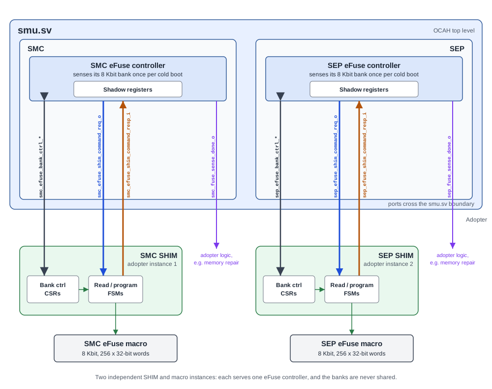
The SMC and the SEP each contain their own eFuse controller, so the smu.sv
boundary carries two independent copies of the interface, one with an smc_
prefix and one with a sep_ prefix. The adopter places two separate SHIM and
macro instances, one per controller, each fronting its own 8 Kbit bank. The
banks are never shared. Each controller also drives its own sense-done output
to the smu.sv boundary, smc_fuse_sense_done_o and sep_fuse_sense_done_o,
and holds the sensed bank in its own shadow registers.
eFuse connections at the smu.sv boundary shows these connections. When the SMU is built with
CFG.SEP = 0, only the SMC instance is needed.
eFuse controller to Interface SHIM contract shows the contract for one of those instances. Everything above the dashed line is provided by OCAH; everything below it is the adopter’s. Only the two interfaces that cross the line are fixed.
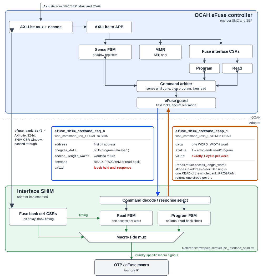
The reference SHIM, hw/ip/efuse/rtl/efuse_interface_shim.sv, drives an
APB-based behavioral bank model. Use it as a worked example of the read and
program state machines, not as a template for macro-side timing.
SHIM control address window. The SHIM control CSRs are defined by the
adopter, but their addresses sit at the base of the subsystem’s adopter
external window. The fabric carves that block off the window and routes it
to the eFuse controller instead of the external port. The controller does not
decode it; it forwards every access outside its own register blocks to
efuse_bank_ctrl unchanged. The rest of the external window leaves on the
subsystem’s external port as usual.
| Subsystem | Window base | Size parameter (SMU default) | Rest of the window |
|---|---|---|---|
SMC |
|
|
|
SEP |
|
|
|
The SHIM must follow these rules for this window:
-
Fit the window. Size the parameter to cover every SHIM control register. Accesses past it go to the external port and never reach the SHIM.
-
Describe the registers in the external map. Place the SHIM control block at offset
0x0of the adopter’ssmc_externalandsep_externalregister maps. The open SMC map reserves the whole window as opaque memory. SEP takes the window base from theefuse_shim_ctrlinstance insep_external, so an adopter map that replaces it must keep an instance of that name at offset0x0.
The reference register block is efuse_shim_ctrl
(hw/ip/efuse/dv/models/regs/efuse_shim_ctrl.rdl), which holds a single
EFUSE_BANK_INIT_TIME register.
The command and response payloads are exchanged as packed structs:
// Controller -> SHIM
typedef struct packed {
    addr_t                address;             // Target address (in bits)
    logic                 program_data;        // Data to program (when programming)
    access_length_words_t access_length_words; // Number of WORD_WIDTH words to access
    command_t             command;             // READ / PROGRAM / PROGRAM_READ_BACK
    logic                 valid;               // Request valid
} fuse_command_req_t;

// SHIM -> Controller
typedef struct packed {
    data_t data;   // Read data (one WORD_WIDTH word)
    logic  status; // Operation status (0 = OK, 1 = error)
    logic  valid;  // Response valid (qualifies `data` for one cycle)
} fuse_command_resp_t;
command is efuse_pkg::fuse_command_e: FUSE_COMMAND_READ (2'b00),
FUSE_COMMAND_PROGRAM (2'b01) and FUSE_COMMAND_PROGRAM_READ_BACK
(2'b10).
The SHIM implements two operations, reads and programs:
-
Reads. If a request has
commandset toFUSE_COMMAND_READandaccess_length_wordsset to N, respond with Nvalidstrobes, each carrying oneWORD_WIDTHword indata, reading consecutive words starting ataddress. Firmware reads set N to one; fuse sensing sets it to the whole bank, as described below. -
Programs. If a request has
commandset toFUSE_COMMAND_PROGRAM, program the single bit ataddressand respond with onevalidstrobe when the macro finishes.program_datais always 1 andaccess_length_wordsis always 1. ForFUSE_COMMAND_PROGRAM_READ_BACK, also read the word back, return it indata, and setstatusif the programmed bit did not stick.
Both operations follow these rules:
-
Bit addressing.
addressis a bit address. Convert it to whatever word or byte addressing the macro uses; the reference SHIM shifts it right by three. -
One command at a time.
validis a level, not a strobe. The controller holdsvalidand the whole request payload stable from the cycle it issues a command until it has received the response, so the SHIM may sample the payload at any point while the command runs. -
When
validfalls. After a firmware read or program,validfalls in the cycle after the response strobe. After sensing it stays high untilfuse_sense_donemoves the arbiter to the firmware path, two cycles after the last strobe; do not treat that still-asserted request as a second read. The controller also withdrawsvalidwithout waiting for a response in these cases, and the SHIM must abandon the command it had started:-
a firmware read or program timeout expires*
-
firmware changes the read or program enable, where program takes priority over read*
-
-
Errors. Setting
statusends a firmware read or program command with an error. The sense FSM counts onlyvalidstrobes, so a sensing error must still be followed by the remaining strobes. -
No access control. The eFuse guard zeroes requests to locked fields, and every request while the SEP is in secure test mode, in the same cycle the request is issued. A blocked request therefore never reaches the SHIM:
validdoes not rise, and no response is expected. Secure test mode is latched once per cold boot, before any firmware command can be issued, so it cannot begin in the middle of a command. The SMC controller has no secure test mode.
* These scenarios will be fixed in a future release so that the
controller never withdraws valid before the response.
|
Fuse sensing happens once per cold boot, when the eFuse controller’s primary reset is released. It runs in both eFuse controller instances, SMC and SEP, each against its own bank. CPU and warm resets do not repeat it. The adopter must provide 8 Kbit of fuses (8192 bits, 256 32-bit words) for
each instance: one bank behind the SMC SHIM and a second, separate bank
behind the SEP SHIM. For both, |
Fuse sensing protocol. During automatic sensing the controller issues a
single read with access_length_words set to the entire bank:
NumShadowWords, which is SHADOW_REG_BITS / WORD_WIDTH. The SHIM is expected
to stream the bank back one WORD_WIDTH word at a time: for each OTP access it
drives the read data onto efuse_shim_command_resp_i.data and asserts
valid for exactly one cycle. The controller consumes one word per cycle
that valid is high, advancing to the next eFuse word on each assertion.
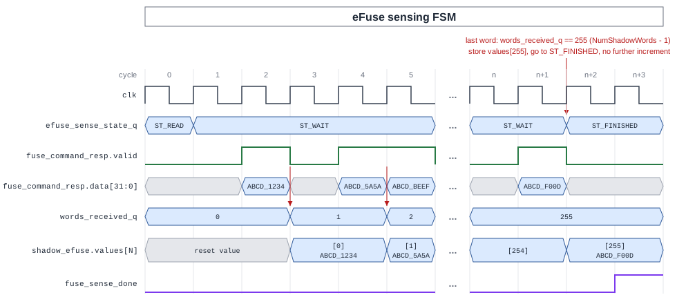
eFuse sensing response stream shows the stream for the 256-word bank. The sense FSM
leaves ST_READ after one cycle and waits in ST_WAIT. Each valid strobe
stores data into shadow word words_received_q and increments the count one
cycle later. Gaps between strobes are allowed, as between cycles 2 and 4, and
so are strobes on consecutive cycles, as in cycles 4 and 5, provided each
cycle carries a new word. data is sampled only while valid is high. The
strobe for word 255 (NumShadowWords - 1) stores the last word and moves the
FSM to ST_FINISHED without incrementing. fuse_sense_done rises one cycle
after that.
|
|
During cold boot the SMC and SEP each sense their own bank into their own
shadow registers. smc_fuse_sense_done_o and sep_fuse_sense_done_o indicate
when each sensing operation completes.
The smc_shadow_regs_o output gives adopter read-only access to the
sensed SMC bank. The SMU has no equivalent SEP output: the SEP bank holds
secrets such as the class key and device UIDs, so its shadow registers stay
inside SEP.
7. Memory Subsystem Integration
The SMC includes an embedded RISC-V CPU cluster with associated memory interfaces. See Immutable ROM FW Integration for the ROM FW integration contract.
7.1. SRAM and Cache Array Integration
Scratch RAM interfaces (smc_scratch_ram_intf_req_o and smc_scratch_ram_intf_rsp_i)
connect to 32 independent RAM banks totaling the scratchpad memory space. Cache
memory interfaces for L1 instruction and data caches (smc_l1_icache_* and
smc_l1_dcache_*) connect to tag and data RAM banks as specified in the port table.
The smc_disable_sram_auto_init_i input controls automatic memory initialization
behavior. When deasserted, the SMC automatically zeroes all SRAM contents during
bring-up. The smc_init_mem_done_o output indicates completion of this
initialization sequence. The SRAM_AUTO_ZERO_DISABLE strap
(STRAPS_LO[26]) can
disable this automatic zeroing behavior if your integration requires preserved
SRAM contents across resets.
8. Memory Repair Integration
The SMC implements Built-In Redundancy Analysis (BIRA) memory repair to address manufacturing defects in SRAM arrays. Repair uses redundant memory elements configured with data stored in eFuse memory, replacing defective cells detected during manufacturing test.
Memory repair executes automatically during boot after eFuse sensing completes and before MBIST operations. The process must complete successfully before the CPU cluster can safely access SRAM arrays. Repair is required on every cold reset but can be bypassed during Function Level Reset (FLR) operations for faster recovery.
8.1. Control Signals
-
smc_fuse_sense_done_o: eFuse controller output indicating fuse sensing completion. External DFT logic monitors this signal to trigger repair operations. -
skip_mem_repair_o: Reset unit output indicating repair should be bypassed. It is driven by the isolation request inputs (isolate_req_pin_sync_smcor the SMC isolation register), not directly by the strap. When asserted, external repair logic should skip operations and immediately assert completion status. -
ext_boot_seq_done_i: External input indicating the boot sequence (memory repair and shadow register override) is complete. Hold low to pause reset release until external logic gives the go-ahead; required before the system can continue its boot sequence.
8.2. Repair Data
The SMC fuse map does not allocate storage for repair data. Your external memory repair controller must source it from wherever your manufacturing flow keeps it and apply it to SRAM arrays according to your memory architecture.
8.3. Status Monitoring
Repair completion and success are reported through
DFX_CTRL_STATUS.STATUS_SMU at 0xC000_B800. The mem_repair_done bit
indicates completion regardless of success, while mem_repair_success indicates
successful repair. Both bits are set by the external repair controller. The SMC
ROM FW monitors these bits during initialization to verify repair
completion.
8.4. Bypass Configuration
The BYPASS_SRAM_REPAIR configuration strap is reported in STRAPS_LO[13]
of the strap registers in the adopter peripheral window. Keep these three mechanisms distinct:
-
No RTL path drives
skip_mem_repair_ofrom this strap directly.skip_mem_repair_ois driven from the isolation request path. -
Production ROM reads the strap and, when asserted, skips repair-status validation and writes
MBIST_STATUS_MEM_REPAIR_BYPASSEDto scratchpad register 15 (SMC_SCRATCH_MBIST_STATUS,0xC003_90F8). It does not cause the external repair controller to skip physical repair. -
External repair logic independently honors
skip_mem_repair_oto decide whether to bypass physical repair operations.
Use bypass mode only when SRAM arrays are guaranteed defect-free, such as during development or with known-good components.
8.5. Integration Requirements
Provide an external memory repair controller that monitors
smc_fuse_sense_done_o to initiate repair, respects skip_mem_repair_o for
bypass control, reads repair data from eFuse shadow registers, applies repair
configuration to SRAM arrays, asserts ext_boot_seq_done_i and updates
DFX_CTRL_STATUS with completion status. The controller operates independently
of the SMC core and must complete before the CPU cluster accesses SRAM.
Note: For a standalone SEP, the adopter must synchronize ext_boot_seq_done_i to
the system clock and ensure the signal is held until next cold reset.
For direct access to the eFuse not through the SHIM, i.e. from a DFT fuse controller, adopters must ensure the integrated logic will not interfere with accesses from the OCAH’s efuse interface.
The isolation request path asserts skip_mem_repair_o during Function Level
Reset (FLR) operations to bypass repair for rapid reset sequences. Normal cold
reset sequences always execute repair unless isolation is already asserted.
9. Interrupt Integration
The SMC aggregates interrupts from multiple sources into cpu_interrupts_o, which feeds
the PLIC of the embedded RISC-V CPU cluster. The interrupt vector is assembled in
hw/sys/smc/rtl/smc_base.sv and
hw/sys/smc/rtl/smc_peripherals/rtl/smc_peripherals.sv. The authoritative
bit-level map (RTL trace and PLIC source ID note) is
maintained in a single place:
The SMC PLIC and CPU interrupt vector are internal. sync_irq_o is not the
interrupt aggregate — it is the software-controlled SYNC_REG.sync global
synchronization bit in the reset unit, unrelated to PLIC interrupt delivery.
Do not connect an external interrupt controller to sync_irq_o.
External interrupt sources visible to the adopter are smc_ext_interrupts_i (SMC
external interrupt input vector, width NUM_INT_TO_SMC),
smc_ext_mailbox_interrupts_o (outbound mailbox notifications, width
NumMailboxes), gpio_interrupt_o (GPIO edge/level events, width
NumGpioWraps), and uart_interrupt_o (UART TX/RX events, width NumUart).
Drive smc_ext_interrupts_i as an active-high level or as a pulse that stays
high long enough to be sampled on clk_smc. The pin is three-flop
synchronized; a short asynchronous pulse can be lost. There is no
edge-triggered mode. For the full PLIC source map see the SMC Technical
Reference Manual.
10. Telemetry and Debug Integration
For system-level debug and telemetry, the SMC implements ATB (Advanced Trace Bus) receiver
interfaces. The telemetry interface group (telemetry_atdata_i, telemetry_atid_i,
telemetry_atvalid_i, telemetry_atready_o) operates in a dedicated clk_telemetry_i
clock domain with separate rst_telemetry_ni reset. Connect these signals to ATB trace
sources for debug data collection.
At the SMC boundary, ext_debug_bus_i is 512 bits wide; the SMU concatenates
the adopter-visible 128-bit input with the SEP’s internal 384-bit bus before
driving SMC. The typed xtrigger_ss_i / xtrigger_ss_o ports are the only
cross-trigger signals at the SMC boundary. The adopter-visible SMU cross-trigger
interfaces are xtrig_ctm_*, xtrig_clk_stop_req_i, and the CTP groups.
Trace memory interfaces (trace_mem_req_o and trace_mem_resp_i) connect to trace RAM
instances for storing captured debug data. smc_ip_integration.sv shows an example set of
RAM instances that can be adapted to your debug requirements.
11. Bring-Up Sequence
The recommended bring-up sequence begins with asserting rst_cold_ni while stabilizing
power supplies and clocks. Once all supplies reach nominal voltages, deassert rst_cold_ni
to initiate the SMC boot sequence. The SMC immediately begins fuse sensing to read configuration
values and security credentials.
Monitor the smc_fuse_sense_done_o signal to detect completion of fuse sensing. The configuration
straps the boot ROMs read determine boot modes and operational settings. After fuse
sensing completes, the SMC releases internal subsystem resets based on the programmed reset
sequencing configuration.
The CPU cluster begins executing the ROM FW after reset release. The ROM FW
performs additional initialization including peripheral configuration, memory
testing (unless disabled), and system health checks. The smc_init_mem_done_o
signal indicates completion of memory initialization if automatic SRAM zeroing
is enabled.
To support Function Level Reset (FLR), assert cfg_flr_pf_active_i to trigger a
warm reset sequence. The SMC asserts isolate_req_o bits for the affected
subsystem indices. The adopter’s power controller drives ss_reset_complete_i
high once the subsystem reset is complete; the SMC synchronizes this into the
readable SS_RESET_COMPLETE register. Isolation remains asserted until cleared
by software: SMC firmware must poll SS_RESET_COMPLETE and then write
ISOLATE_REQ_SMC_REG to clear the FLR isolation latch. Do not assume isolation
releases automatically on ss_reset_complete_i.
See hw/top/smu_wrapper.sv and hw/top/smc_ip_integration.sv for reference
bring-up wiring examples covering clock, reset, strap, and peripheral connections.
12. SMC Port Interface
The SMC exposes a comprehensive set of interfaces for system integration. The following table defines all SMC top-level ports including clocks, resets, AXI interfaces, peripheral connections, and control signals. Refer to the detailed SMC documentation for internal signal descriptions and timing requirements.
The generated module and port pages are in the TRM under RTL Modules Reference. This table keeps each port’s connection and tie-off default.
| Interface Name | Type | Direction | Width | Description | Connection | Default value (if applicable) |
|---|---|---|---|---|---|---|
|
|
Input |
1 |
Primary SMC clock domain. All SMC internal logic operates synchronously to this clock. |
PLL output |
N/A |
|
|
Input |
1 |
Reference clock domain. Used for timing-sensitive operations and peripheral interfaces. |
PLL reference clock |
N/A |
|
|
Input |
1 |
Peripheral clock domain. |
PLL peripheral clock |
N/A |
|
|
Input |
1 |
Power-good indication. Assert after supply voltages stabilize. |
Power management controller |
N/A |
|
|
Output |
1 |
Stabilized power-good output. Debounced version of |
Reset unit → External systems |
N/A |
|
|
Input |
1 |
Cold reset input (active low). Assertion and deassertion are synchronous to |
System cold reset |
N/A |
|
|
Output |
1 |
Primary reset synchronized to reference clock domain (active low). |
To subsystems using ref clock |
N/A |
|
|
Output |
1 |
Primary reset synchronized to SMC clock domain (active low). |
To subsystems using SMC clock |
N/A |
|
|
Input |
- |
System AXI input request (56-bit addr, 64-bit data, 6-bit ID, 12-bit user). |
External system masters → Input Fabric |
N/A, tie to '0 if unused |
|
|
Output |
- |
System AXI input response. |
Input Fabric → External system masters |
N/A, leave floating if unused |
|
|
Input |
- |
JTAG debug AXI request (56-bit addr, 64-bit data, 2-bit ID, 12-bit user). |
JTAG debug port → Input Fabric |
N/A, tie to '0 if unused |
|
|
Output |
- |
JTAG debug AXI response. |
Input Fabric → JTAG debug port |
N/A, leave floating if unused |
|
|
Input |
- |
eFuse OTP/JTAG AXI-Lite request. |
JTAG → eFuse controller |
N/A, tie to '0 if unused |
|
|
Output |
- |
eFuse OTP/JTAG AXI-Lite response. |
eFuse controller → JTAG |
N/A, leave floating if unused |
|
|
Input |
- |
SEP AXI request (56-bit addr, 64-bit data, 6-bit ID, 12-bit user). |
SEP → Input Fabric |
N/A, tie to '0 if unused |
|
|
Output |
- |
SEP AXI response. |
Input Fabric → SEP |
N/A, leave floating if unused |
|
|
Output |
- |
Filtered and remapped AXI output request (56-bit addr, 64-bit data, 8-bit ID, 12-bit user). |
Output Fabric → External system resources |
N/A, leave floating if unused |
|
|
Input |
- |
Filtered and remapped AXI output response. |
External system resources → Output Fabric |
N/A, tie to '0 if unused |
|
|
Output |
- |
eFuse bank control AXI-Lite request. |
eFuse controller → eFuse Shim |
N/A |
|
|
Input |
- |
eFuse bank control AXI-Lite response. |
eFuse Shim → eFuse controller |
N/A |
|
|
Output |
- |
eFuse command interface request. |
eFuse controller → eFuse Shim |
N/A |
|
|
Input |
- |
eFuse command interface response. |
eFuse Shim → eFuse controller |
N/A |
|
|
Output |
- |
eFuse shadow register output. |
eFuse controller → External systems |
N/A |
|
|
Input |
1 |
PLL clock observation input. |
PLL → GPIO padring (muxed) |
N/A |
|
|
Input |
1 |
PLL clock observation enable. |
Control logic → GPIO padring |
N/A |
|
|
Input |
1 |
PVT process monitor clock observation input. |
PVT → GPIO padring (muxed) |
N/A |
|
|
Input |
1 |
PVT process monitor clock observation enable. |
Control logic → GPIO padring |
N/A |
|
|
Input |
1 |
CAT thermal sensor input. |
CAT thermal sensor → PVT wrap |
N/A, tie to '0 if unused |
|
|
Output |
|
LSIO interface selection for each GPIO wrap. |
GPIO padring → GPIO wraps |
N/A |
|
|
Input |
|
GPIO input data from pad ring to core. |
GPIO padring → SMC |
N/A |
|
|
Output |
|
GPIO output data from core to pad ring. |
SMC → GPIO padring |
N/A |
|
|
Output |
|
GPIO pad-to-core path enable. |
SMC → GPIO padring |
N/A |
|
|
Output |
|
GPIO core-to-pad path enable. |
SMC → GPIO padring |
N/A |
|
|
Input |
1 |
Cool reset input from GPIO pin 61. |
GPIO pin 61 → Reset Unit |
N/A |
|
|
Input |
1 |
Telemetry clock domain. Separate clock for ATB telemetry data collection. |
Telemetry clock source |
N/A |
|
|
Input |
1 |
Telemetry reset (active low). Resets telemetry receiver logic. |
Telemetry reset source |
N/A |
|
|
Input |
|
ATB telemetry data input array. |
ATB sources → Telemetry receivers |
N/A |
|
|
Input |
|
ATB telemetry ID input array. |
ATB sources → Telemetry receivers |
N/A |
|
|
Output |
|
ATB telemetry ready output. |
Telemetry receivers → ATB sources |
N/A |
|
|
Input |
|
ATB telemetry valid input. |
ATB sources → Telemetry receivers |
N/A |
|
|
Output |
|
ATB flush valid output. |
Telemetry receivers → ATB sources |
N/A |
|
|
Input |
|
ATB flush ready input. |
ATB sources → Telemetry receivers |
N/A |
|
|
Output |
1 |
Cluster double error detection output. |
CPU cluster → External systems |
N/A |
|
|
Output |
1 |
First watchdog timeout signal. |
CPU cluster WDT → Reset Unit |
N/A |
|
|
Output |
1 |
Second watchdog timeout signal. |
Reset Unit → External systems |
N/A |
|
|
Output |
|
SMC address region size output. |
SMC Internal Registers → External systems |
N/A |
|
|
Input |
|
External interrupt inputs. Width is 256. Active-high level or a pulse long enough to be sampled on |
External sources → Interrupt aggregator |
N/A, tie to '0 if unused |
|
|
Input |
|
SEP → SMC mailbox interrupt inputs (8 channels). Routed to internal interrupts to the SMC CPU. |
SEP → Interrupt aggregator |
N/A, tie to '0 if unused |
|
|
Input |
1 |
SEP watchdog reset (active low). Active-low polarity is inverted before routing to internal interrupts to the SMC CPU. |
SEP → Interrupt aggregator |
N/A |
|
|
Output |
1 |
Fuse sense completion output. |
eFuse controller → Memory repair logic |
N/A |
|
|
Output |
1 |
Delayed fuse reset output (after 16 pipeline stages). |
eFuse controller → External systems |
N/A |
|
|
Output |
1 |
Skip memory repair output. |
Reset Unit → Memory repair logic |
N/A |
|
|
Input |
1 |
Asynchronous external boot sequence completion (memory repair and shadow register override done). Qualified in |
External boot/repair controller → SMC peripherals |
N/A |
|
|
Input |
|
Lifecycle state input, differentially encoded. |
Lifecycle controller → SMC Internal Registers |
From SEP; tie to 8’hf0 if unused (encoded TEST_DEV) |
|
|
Output |
|
External mailbox interrupt outputs (32 interrupts, mapped to IDs 156-187). |
Mailbox controller → External targets |
N/A |
|
|
Input |
1 |
Function Level Reset (FLR) PF active signal. |
PCIe/System → Reset Unit |
N/A, tie to '0 if unused |
|
|
Input |
|
NDM reset request from external CPU cluster |
External CPU clusters → SMC |
Tie to '0 if unused |
|
|
Output |
|
Firmware response to external CPU cluster |
SMC → external CPU clusters |
N/A |
|
|
Output |
|
Isolation request output for 32 subsystems. |
Reset Unit → 32 subsystems |
N/A |
|
|
Input |
|
Subsystem reset completion status. |
32 subsystems → Reset Unit |
32’hFFFFFFFF |
|
|
Output |
|
Subsystem configuration output. |
Reset Unit → 32 subsystems |
N/A |
|
|
Output |
|
Subsystem reset control output array. |
Reset Unit → 32 subsystems |
N/A |
|
|
Output |
1 |
Software-controlled global synchronisation bit ( |
Reset unit → External |
N/A |
|
|
Output |
|
Raw GPIO interrupt vector from the padring, one bit per GPIO wrap (bonded + unbonded). Software reads GPIO status registers to identify the interrupt source. Already OR-reduced into |
|
N/A, leave floating if unused |
|
|
Output |
|
Raw UART interrupt outputs, one bit per UART instance, in the peripheral clock domain. Already aggregated into |
|
N/A, leave floating if unused |
|
|
Output |
- |
ROM memory interface request. Width depends on CPU cluster configuration |
CPU cluster → Boot ROM |
N/A |
|
|
Input |
- |
ROM memory interface response. Width depends on CPU cluster configuration |
Boot ROM → CPU cluster |
N/A |
|
|
Output |
|
Scratch RAM interface requests. Width depends on CPU cluster configuration |
CPU cluster → Scratch RAM banks |
N/A |
|
|
Input |
|
Scratch RAM interface responses. Width depends on CPU cluster configuration |
Scratch RAM banks → CPU cluster |
N/A |
|
|
Output |
|
L1 I-cache tag interface requests. Width depends on CPU cluster configuration |
CPU cluster → L1 I-cache tag banks |
N/A |
|
|
Input |
|
L1 I-cache tag interface responses. Width depends on CPU cluster configuration |
L1 I-cache tag banks → CPU cluster |
N/A |
|
|
Output |
|
L1 I-cache data interface requests. Width depends on CPU cluster configuration |
CPU cluster → L1 I-cache data banks |
N/A |
|
|
Input |
|
L1 I-cache data interface responses. Width depends on CPU cluster configuration |
L1 I-cache data banks → CPU cluster |
N/A |
|
|
Output |
|
L1 D-cache tag interface requests. Width depends on CPU cluster configuration |
CPU cluster → L1 D-cache tag banks |
N/A |
|
|
Input |
|
L1 D-cache tag interface responses. Width depends on CPU cluster configuration |
L1 D-cache tag banks → CPU cluster |
N/A |
|
|
Output |
|
L1 D-cache data interface requests. Width depends on CPU cluster configuration |
CPU cluster → L1 D-cache data banks |
N/A |
|
|
Input |
|
L1 D-cache data interface responses. Width depends on CPU cluster configuration |
L1 D-cache data banks → CPU cluster |
N/A |
|
|
Input |
1 |
Disable SRAM automatic initialization. |
Control logic → CPU cluster |
1’b0 |
|
|
Output |
1 |
Memory initialization completion signal. |
CPU cluster → Control logic |
N/A |
|
|
Input |
1 |
Chiplet is primary signal. Used for System Timer OCTS |
|
N/A |
|
|
Output |
|
64-bit system timer count output for Open Chiplet Time Synchronization (OCTS). |
System Timer OCTS → External systems |
N/A |
|
|
Input |
- |
Typed reset-override control struct carrying all SMC reset override enables and active-low values. Driven by DTP via JTAG IC_RESET. Tie all enables to 0 when not used. |
DTP → SMC reset unit |
All enables 0 |
|
|
Output |
1 |
CLA GPIO enable output. |
DFD controller → CLA |
N/A |
|
|
Input |
1 |
DEBUG_CONTROL CLA clock-stop enable. |
DTP → DFD |
1’b0 |
|
|
Output |
1 |
CLA halt-clock status under enable; also drives |
DFD → DTP / interrupt |
N/A |
|
|
Input |
- |
Cross-trigger subsystem input. SMU drives from |
SMU internal: DTP |
N/A |
|
|
Output |
- |
Cross-trigger subsystem output. SMU routes to |
SMU internal: SMC → DTP |
N/A |
|
|
Output |
|
Trace memory interface requests. |
DFD controller → Trace memory |
N/A, leave floating if unused |
|
|
Input |
|
Trace memory interface responses. |
Trace memory → DFD controller |
N/A, tie to '0 if unused |
|
|
Input |
|
External debug bus input (512 bits, 16-bit aligned). |
External debug sources → Debug bus aggregator |
N/A, tie to '0 if unused |
|
|
Input |
1 |
DFT/scan test-enable. Drives clock-gater test ports and AXI cell test inputs. |
Test controller → All modules |
1’b0 |
|
|
Input |
1 |
Scan reset (active-low). Bypasses reset synchronizers during DFT. |
Test controller → All modules |
1’b1 |
13. GPIO Pin Requirements
The SMC provides GPIO functionality with multiplexed peripheral functions and
test interfaces. The following table lists each pad’s index, assigned
function, recommended pull, and GPIO-specific notes. It does not define
default direction or decode configuration straps; use
smc_padring_pkg::DefaultDirectionMap and the STRAPS_LO and STRAPS_HI
register descriptions (see Mandatory Region) for those.
| Index | Function | Recommended Pull | GPIO Notes |
|---|---|---|---|
0 |
SPI.DATA[0] |
PD |
|
1 |
SPI.DATA[1] |
PD |
|
2 |
SPI.DATA[2] |
PD |
|
3 |
SPI.DATA[3] |
PD |
|
4 |
SPI.DATA[4] |
PD |
|
5 |
SPI.DATA[5] |
PD |
|
6 |
SPI.DATA[6] |
PD |
|
7 |
SPI.DATA[7] |
PD |
|
8 |
SPI.CS |
PU |
|
9 |
SPI.CLK |
PD |
|
10 |
SPI.DQS |
PD |
|
11 |
UART[0].RX |
PU |
|
12 |
UART[0].TX |
PU |
|
13 |
UART[0].RTS |
PD |
|
14 |
UART[0].CTS |
PD |
|
15 |
UART[1].RX |
PU |
|
16 |
UART[1].TX |
PU |
|
17 |
UART[1].RTS |
PD |
|
18 |
UART[1].CTS |
PD |
|
19 |
UART[2].RX |
PU |
|
20 |
UART[2].TX |
PU |
|
21 |
UART[2].RTS |
PD |
|
22 |
UART[2].CTS |
PD |
|
23 |
UART[3].RX |
PU |
|
24 |
UART[3].TX |
PU |
|
25 |
UART[3].RTS |
PD |
|
26 |
UART[3].CTS |
PD |
|
27 |
I3C[0] SCL |
PU |
|
28 |
I3C[0] SDA |
PU |
|
29 |
I3C[2] SCL |
PU |
|
30 |
I3C[2] SDA |
PU |
|
31 |
I3C[3] SCL |
PU |
|
32 |
I3C[3] SDA |
PU |
|
33 |
I3C[4] SCL |
PU |
|
34 |
I3C[4] SDA |
PU |
|
35 |
I3C[5] SCL |
PU |
|
36 |
I3C[5] SDA |
PU |
|
37 |
I2C[0] SCL |
PU |
Every I2C can be programmed to act as I2C, SMBus or PMBus |
38 |
I2C[0] SDA |
PU |
|
39 |
I2C[0] SMB_A |
PU |
SMBus Alert |
40 |
I2C[0] SMB_D |
PU |
SMBus Suspend |
41 |
I2C[1] SCL |
PU |
|
42 |
I2C[1] SDA |
PU |
|
43 |
I2C[1] SMB_A |
PU |
SMBus Alert |
44 |
I2C[1] SMB_D |
PU |
SMBus Suspend |
45 |
I2C[2] SCL |
PU |
|
46 |
I2C[2] SDA |
PU |
|
47 |
I2C[2] SMB_A |
PU |
SMBus Alert |
48 |
I2C[2] SMB_D |
PU |
SMBus Suspend |
49 |
AVS.CLOCK |
PU |
|
50 |
AVS.MDATA |
PU |
|
51 |
AVS.SDATA |
PU |
|
52 |
Thermal Emergency N |
PU |
|
53 |
Isolate Request |
PD |
|
54 |
SPI DQS Loopback |
PD |
|
55 |
System Timer Sync Load |
PD |
|
56 |
System Timer Credit Count |
PD |
|
57 |
Boot Stall |
PD |
Stall after fuse sensing to override shadow register values. Boot will resume when this GPIO is released. This value can be overridden by the value specified over JTAG using the boot_stall_jtag_ovrd and boot_stall_jtag_val signals from DTP. |
58 |
OCCP Interface |
PD |
|
59 |
Reserved |
PD |
|
60 |
Reserved |
PD |
|
61 |
Cool Reset In |
PU |
Not packaged out |
62 |
Cool Reset Out |
PU |
Not packaged out |
63 |
I3C[1] SCL |
PU |
Not packaged out |
64 |
I3C[1] SDA |
PU |
Not packaged out |
65 |
PTAP TCK |
No dedicated interface in harness |
|
66 |
PTAP TRST |
No dedicated interface in harness |
|
67 |
PTAP TDI |
No dedicated interface in harness |
|
68 |
PTAP TMS |
No dedicated interface in harness |
|
69 |
PTAP TDO |
No dedicated interface in harness |
|
70 |
STAP TCK |
No dedicated interface in harness |
|
71 |
STAP TRST |
No dedicated interface in harness |
|
72 |
STAP TDI |
No dedicated interface in harness |
|
73 |
STAP TMS |
No dedicated interface in harness |
|
74 |
STAP TDO |
No dedicated interface in harness |
|
75 |
BP_REFCLK_VDD_SYS |
No dedicated interface in harness |
|
76 |
BP_RESETN |
No dedicated interface in harness |
|
77 |
BP_POWERGOOD |
No dedicated interface in harness |
For multi-chiplet systems, the PRIMARY_CHIPLET strap (STRAPS_LO[25])
determines whether the chiplet operates as primary or secondary. The primary
chiplet’s System Timer OCTS (Open Chiplet Time Synchronization) generates
synchronization pulses (timer_sync_load_o, timer_cnt_credit_o) that
secondary chiplets receive to maintain coherent timestamps across the system.
The chiplet_is_primary_i input carries this strap and should be held constant
while the SMC is out of cold reset.