Overview
The DTP contains two major functional blocks — the JTAG Interface Unit (JIU) and the Cross Trigger Network (CTN) — plus the DTP top-level wiring that connects them to each other, to the SMC and SEP, and to the external JTAG and cross-trigger pads.
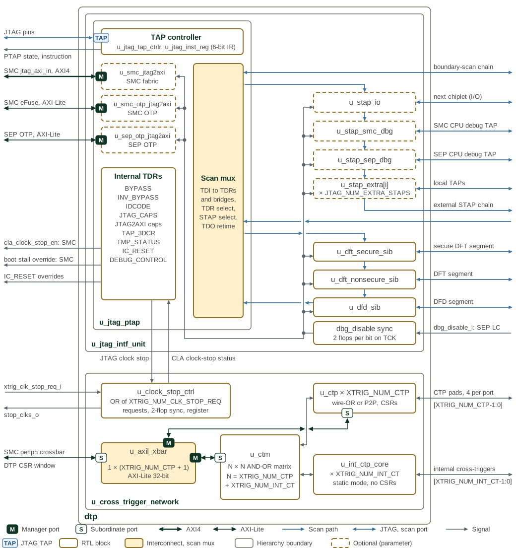
Figure 1 draws each RTL instance under its instance name
inside the u_jtag_intf_unit and u_cross_trigger_network hierarchy boundaries.
Labels at the figure edges name what each DTP port connects to in the SMU. Blue
lines carry JTAG and scan data, dark lines AXI4 and AXI-Lite, and grey lines other
signals. Dashed blocks exist only when their enable parameter is set: the three
JTAG2AXI bridges follow JTAG_SMC_DBG_ENABLE and JTAG_SEP_DBG_ENABLE, and the
STAPs follow JTAG_STAP_IO_ENABLE, JTAG_SMC_DBG_ENABLE, JTAG_SEP_DBG_ENABLE
and JTAG_NUM_EXTRA_STAPS. The grey fan-out from the debug-disable synchroniser
reaches every STAP, SIB and bridge. The
DTP JTAG scan chain figure gives the
serial order of the scan paths.
The figure names each count by its dtp parameter. XTRIG_NUM_CTP external CTPs,
XTRIG_NUM_INT_CT internal lanes and XTRIG_NUM_CLK_STOP_REQ clock-stop requests
default to the dtp_pkg values 16, 10 and 9. The CTM is N × N, where N is
XTRIG_NUM_CTP + XTRIG_NUM_INT_CT (26 by default); its generated register
geometry must equal that sum, which elaboration checks. u_axil_xbar has one
manager port for the CTM and one for each external CTP, 17 by default.
JTAG_NUM_EXTRA_STAPS sets the number of u_stap_extra instances, 1 by default.
In the cross-trigger network, u_axil_xbar decodes the DTP CSR window, which the
SMC peripheral crossbar rebases to 0, onto the CTM at offset 0x000 and one 16-byte
window for each external CTP from 0x200. The internal cross-trigger lanes are
u_int_ctp_core instances without CSRs, whose protocol XTRIG_INT_CT_MODE fixes.
In the SMU the first two lanes connect to the SMC DFD CLA, one clock-stop request
comes from the CLA, and the remaining lanes and requests leave the SMU.
1. JTAG Interface Unit
The JTAG Interface Unit (JIU) is the top-level JTAG control module. It contains:
-
A Primary TAP (PTAP) — the main chiplet JTAG entry point, connected to the five external JTAG pins (TCK, TDI, TDO, TMS, TRST_n).
-
A configurable set of Secondary TAPs (STAPs) — for I/O chiplet-to-chiplet JTAG, SMC CPU debug, SEP CPU debug, and optional extra TAPs.
-
An iJTAG network selected by
SELECT_IJTAG, with a serial cascade of secure DFT, non-secure DFT, and DFD SIBs. Each SIB inserts or bypasses its associated external scan segment. -
Independent instruction-selected PTAP TDRs for SMC fabric debug (JTAG2AXI), SMC OTP (JTAG2AXIL), and SEP OTP (JTAG2AXIL). These bridges are outside the iJTAG SIB cascade.
2. Cross Trigger Network
The Cross Trigger Network (CTN) routes cross-trigger pulses between on-chip sources and sinks and the external CTP pads. It consists of:
-
Cross Trigger Ports (CTPs) — pad-facing modules, each connecting to four I/O pads (CT_Req_out, CT_Ack_in, CT_Req_in, CT_Ack_out) and supporting both wire-OR and point-to-point signalling.
-
Cross Trigger Matrix (CTM) — an N × N AND-OR crossbar (26 × 26 by default) that statically routes trigger pulses under AXI-Lite CSR control.
-
Clock stop aggregation — the CTN OR-reduces all
xtrig_clk_stop_req_iinputs (CLA sources) and OR-combines the result with the JTAGjtag_clock_stopbit to produce the registeredstop_clks_ooutput.
Per-path debug-disable inputs gate STAPs, iJTAG SIBs, and JTAG2AXI bridges.
3. Debug Access Paths
External debug access reaches the DTP subsystem through two routes:
JTAG path: An external debugger drives the five JTAG pins directly. The PTAP decodes the JTAG instruction, selects the appropriate TDR, and routes data through the scan chain. JTAG2AXI instructions allow the debugger to generate AXI transactions on the SMC fabric via the PTAP’s built-in bridges, without involving the SMC CPU.
AXI path: The DTP cross-trigger configuration registers (CTM and CTP CSRs)
are memory-mapped inside the SMC address space. The SMC exposes them on its
axil_dtp_csr_req_o / axil_dtp_csr_resp_i interface, which the SMU wires
directly to the DTP axil_xtrig_req_i / axil_xtrig_resp_o ports. Software
running on the SMC reaches the CTN CSRs through its own register map
(dtp_ctrl_reg in smc.rdl). An external debugger using the PTAP JTAG2AXI
bridge reaches the same window through the SMC fabric AXI port.
See OCAH Memory Map for the SMU
address envelope, and the
CTN Memory Map
section for the CTN-internal address layout.
Firmware and an external debugger share this window. The Programmer’s Guide gives the cross-trigger programming sequence.