Key Manager (KM)
The Key Manager provides isolated key storage, random key generation, explicit revocation, and delivery to the cryptographic accelerators. The following sections describe its hardware architecture and firmware interface.
The immutable ROM firmware first initializes the Key Manager, then remains active to process SEP mailbox commands and service interrupts. It is both startup firmware and the resident runtime; "boot ROM" names the memory, not its only function. On an explicit firmware-load/execute command, ROM can hand control to mutable firmware in SRAM. The Key Manager Application ROM appendix of the Programmer’s Guide defines the implemented services, command protocol and handover rules.
1. Architecture
The Key Manager (KM) uses a PicoRV32 CPU, private memories and a Key and Policy Vault (KPV) to separate key management from SEP host execution. The host submits commands and supplied key material through a mailbox; KM firmware validates requests, accesses the vault and writes accelerator sideload registers. The host has no direct bus access to KM key storage.
The ROM is the resident command processor as well as the startup firmware. Its mailbox commands report the hardware, ROM and SRAM firmware versions and the recoverable-error status, generate keys from the DRBG, load SEP-supplied keys, revoke keys, transfer keys to the accelerators, shred accelerator sideload keys, capture the Adams Bridge ML-KEM shared key into the vault, set cold-domain OTP read-locks, and either load and execute mutable firmware in SRAM or keep the ROM running (the command summary in the Programmer’s Guide).
A single KM-mastered AXI4-Lite crossbar connects KMCSR, KPV, the DRBG sampler and mailbox to the private accelerator key interfaces and the SEP OTP/eFuse access path. The accelerator interfaces serve AES, HMAC, KMAC, OTBN and Adams Bridge. Address decoding separates their windows; command and key policy checks belong to KM firmware.
The Memory Map and Register Reference at the end of the chapter defines the address windows and all generated fields. The Key Manager Application ROM appendix of the Programmer’s Guide defines commands, validation and responses. ROM/SRAM parity detects errors but does not correct them; the ROM fault handler can report an unrecoverable fault and halt the CPU.
Figure 1 shows the Key Manager CPU, vault, mailbox, and accelerator interfaces.
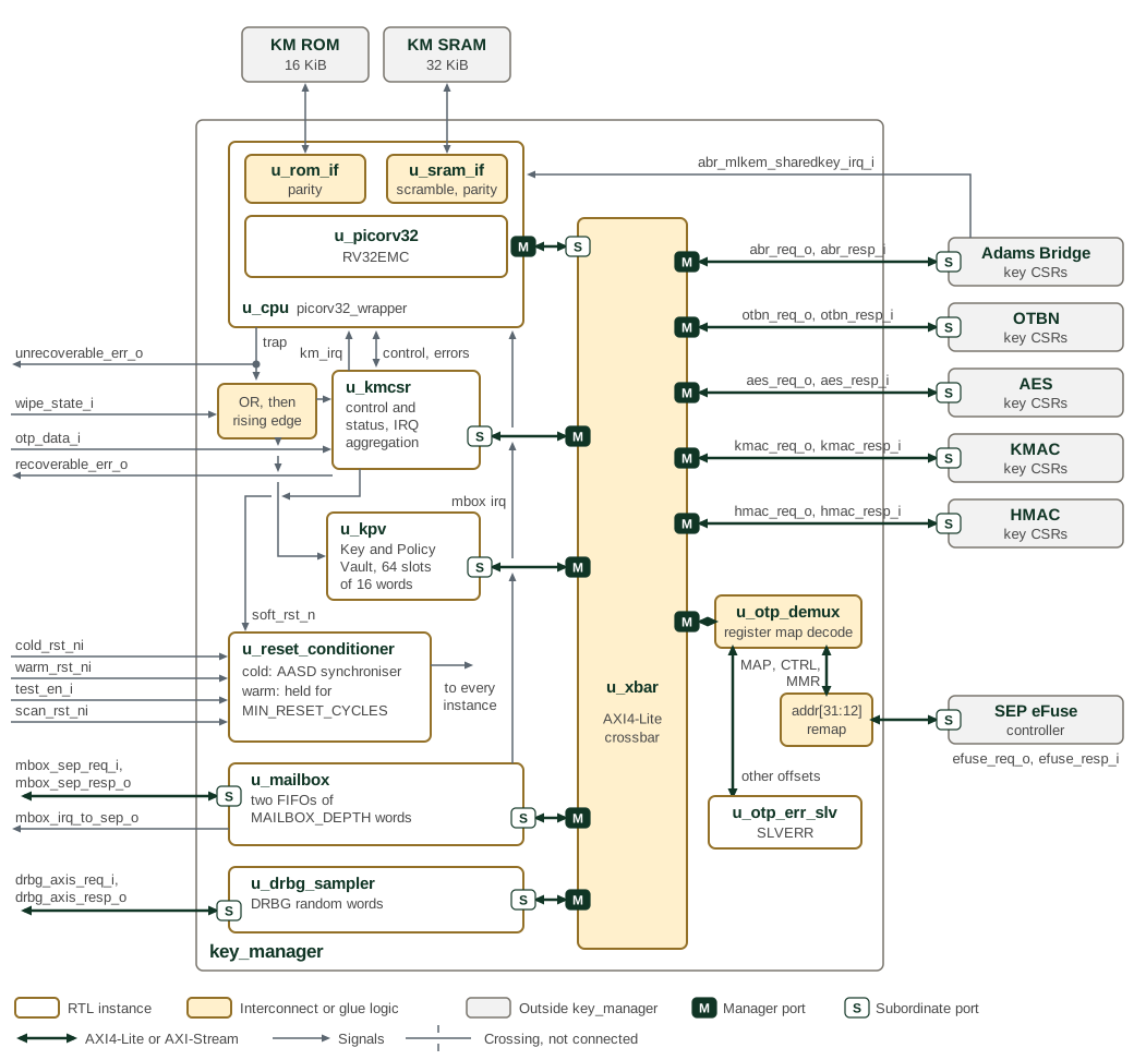
White boxes are key_manager instances, cream boxes are interconnect or glue
logic, and grey boxes lie outside key_manager. M and S mark the manager and
subordinate side of each AXI4-Lite or AXI-Stream connection.
The CPU reaches the ROM and SRAM through direct memory ports rather than the
crossbar. The ROM and SRAM hard macros are instantiated at integration level,
so key_manager exposes rom_mem_* and sram_mem_* ports to them. Every
other CPU access leaves the PicoRV32 AXI4-Lite master and is decoded by
u_xbar.
The five engine ports reach only the key CSRs of each engine wrapper. In SEP
each passes through its own isolation stage and carries no host traffic; the
SEP host reaches the engines' data registers through the crypto interconnect,
a path the KM does not see. For offsets in the MAP, CTRL and MMR register maps,
the OTP/eFuse port replaces address bits [31:12] with
OTP_EFUSE_REMAP_BASE[31:12] before driving efuse_req_o; it answers every
other offset in the window with SLVERR.
A rising edge on wipe_state_i, or a CPU trap, zeroes the KPV and sets
IRQ_STATUS.WIPE_STATE in KMCSR. The CPU trap also drives
unrecoverable_err_o. u_kmcsr drives soft_rst_n into
u_reset_conditioner (Figure 2). test_en_i selects the
scan reset in u_reset_conditioner and drives the test inputs of u_xbar and
u_mailbox.
1.1. Parameters
The Key Manager is configured through its ROM and SRAM sizes, the mailbox FIFO depth,
the read-data behaviour of its memories, and the address of the eFuse controller.
The main KM SRAM is 32 KB (8192 × 32-bit words), implemented with the scrambler macro
scrambler_8192x32. The SRAM macro must return read data (rvalid) at least one cycle
after the cycle in which it grants the read, because the SRAM interface descrambles and
parity-checks each response with the address and byte strobes it captures at the grant.
The parameters of key_manager are listed in key_manager.
1.2. Reset Conditioning
Figure 2 shows how cold and warm reset requests are conditioned for the Key Manager.
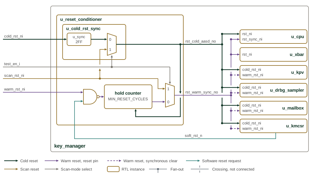
Each reset net keeps its own colour. The cold and warm outputs of
u_reset_conditioner run in two spines beside the instances, with the port
name at each instance edge. A solid warm line drives a reset pin; a dashed warm
line is a synchronous clear, which the instance samples on clk_i rather than
using as a reset. Junction dots mark fan-out, and a gap in a line
marks a crossing without connection. In test mode, test_en_i selects
scan_rst_ni in both scan multiplexers.
Cold and warm resets have different scopes. Warm reset restarts the CPU and its control interfaces while retaining cold-domain state and memory contents. Retention across warm reset does not make SRAM or registers non-volatile, and reset must not be treated as a key-data wipe.
Table 1 identifies the two external reset inputs and their SEP connections.
| Input port | Polarity | Synchronicity | Integration tie-off (SEP) |
|---|---|---|---|
|
Active-low |
Asynchronous |
SEP system cold reset ( |
|
Active-low |
Synchronous to |
SEP KM sub-component software-reset CSR bit ( |
SEP isolates the Key Manager’s AXI paths before asserting the warm reset; see Resetting the Key Manager.
km_reset_conditioner produces two active-low outputs:
-
rst_cold_aasd_no:cold_rst_nipasses throughprim_rst_syncfor asynchronous assertion and synchronous release. There is no cold-path hold counter. Cold reset also asserts the warm path. -
rst_warm_sync_no: either synchronous input,warm_rst_nior KMCSRsoft_rst_ni, triggers a hold counter. Reset remains asserted for at leastMIN_RESET_CYCLESclocks (default 10) after the trigger releases. The cold output asynchronously resets this counter; cold reset is not sampled as a synchronous trigger.
scanmode_i selects scan_rst_ni to override both paths for DFT.
Table 2 identifies resettable state;
it does not imply that key-data flops or memory arrays have reset values.
| Reset domain | Components |
|---|---|
Cold only ( |
ROM/SRAM memory interfaces and parity logic; SRAM scrambler
lock state ( |
Warm + cold ( |
PicoRV32 CPU core; the KM-internal AXI4-Lite crossbar/fabric transaction state; the KMCSR warm subset ( |
The internal AXI4-Lite fabric and generated register CPU interfaces reset on warm reset, discarding their in-flight transaction state. This is an internal reset boundary, not a completion or cancellation guarantee for an external accelerator transaction. Mailbox FIFO contents survive warm reset; ROM flushes the mailbox during boot before accepting new commands.
Writing 0x53525354 (ASCII "SRST") to KMCSR SOFT_RST_CODE triggers the
warm path. BOOT_STATUS.COLD_BOOT_DONE survives it: ROM sets this flag after
cold-boot initialization and reads it on subsequent boots to distinguish
warm restart from cold initialization.
1.3. Mailbox Transport
The mailbox is a raw 32-bit word transport with two FIFOs: inbound SEP-to-KM and outbound KM-to-SEP, each at least 16 words deep. Hardware does not parse commands, validate CRCs or enforce key policy. Firmware defines the framing in Table 3 and Table 4; use the firmware reference for command legality, sequencing and error responses.
| header_crc8[31:24] | message_length[23:16] | function_id[15:8] | sequence_number[7:0] |
|---|---|---|---|
Data_1[31:0] |
|||
Data_2[31:0] |
|||
… |
|||
Data_N[31:0] |
|||
CRC32[31:0] - checksum |
|||
Command/response messages without a data payload (message_length = 0x00) drop the payload CRC32 and only contain the header (Table 4).
| header_crc8[31:24] | 0x00 | function_id[15:8] | sequence_number[7:0] |
|---|
Each FIFO word carries a separator bit that the sender sets on the last word of a message. The receiver uses it with the header length to check framing. Reads pop words; writes push words. Status reports fill level and empty/full conditions.
A write to a full FIFO drops the incoming word without changing queued data. An empty read has no data to consume. Both return SLVERR by default, with configuration allowing OKAY, and set the corresponding sticky overflow or underflow status. Each side has write-one-to-trigger flush control: either side flushes both FIFOs and sets the peer’s flushed-by-other status.
Each side independently enables its interrupt sources. Receive-data-available and transmit-space-available are level conditions; overflow, underflow and peer-flush are sticky conditions. Their enabled OR drives one interrupt to each side: directly to the KM CPU for the KM side, and to the SEP interrupt controller for the SEP side. KM firmware validates received words before executing a command and uses the outbound FIFO for responses and fault notifications. Error handling and resynchronization are firmware operations, not hardware command filtering.
Figure 3 shows the mailbox paths used for SEP commands and Key Manager responses.
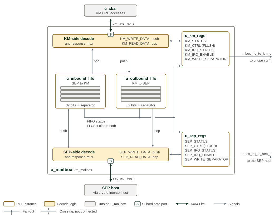
The KM CPU enters at the top and the SEP host at the bottom. Each side’s
decode sends its WRITE_DATA address to a FIFO push and its READ_DATA
address to a FIFO pop, and every other address to its own register block.
Words therefore travel upwards through u_inbound_fifo and downwards through
u_outbound_fifo. Each register block reads the status of both FIFOs, and a
FLUSH from either block clears both of them. MAILBOX_DEPTH sets the depth
of each FIFO; SEP instantiates the KM with 16 words.
1.4. Key Delivery
Keys reside in the KPV and reach accelerator sideload registers through the KM-mastered key path. Host-supplied material enters through mailbox commands; generated secret material is not returned through a direct host read path. The generated Section 3.1 defines the KM’s allocated windows.
Figure 4 separates the key-delivery path on the top row from the host-accessible data path on the bottom row. This separation does not establish resistance to physical fault injection or side-channel attacks. Firmware’s key-data CRC detects corruption; it is not a substitute for access control or a physical-attack guarantee.
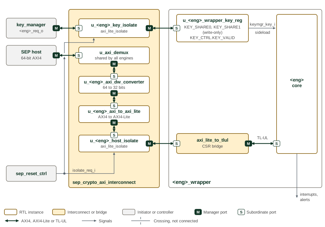
The figure shows one engine wrapper; <eng> stands for otbn, aes, kmac
or hmac. The KM port for that engine (otbn_req_o, aes_req_o,
kmac_req_o or hmac_req_o) is a point-to-point 32-bit AXI4-Lite path. It
passes only through u_<eng>_key_isolate in sep_crypto_axi_interconnect,
which drains the path when sep_reset_ctrl requests isolation, and ends on the
wrapper’s generated <eng>_wrapper_key_reg block. The KEY_SHARE0 and
KEY_SHARE1 words are write-only, and reads return zero. The two shares and
KEY_CTRL.KEY_VALID drive the engine’s keymgr_key_i sideload port; the XOR
of the two shares is the key. The shares are 8 words each, or 12 words for
OTBN.
The SEP host reaches the engine’s own registers on a separate path: the
crypto interconnect demultiplexes the 64-bit AXI4 host bus in u_axi_demux,
converts it to 32 bits in u_<eng>_axi_dw_converter and to AXI4-Lite in
u_<eng>_axi_to_axi_lite, and passes it through u_<eng>_host_isolate, and the
wrapper bridges it to the engine’s TL-UL port. isolate_req_i from
sep_reset_ctrl drives both isolation stages. The host path does not reach
the key registers, and the KM path does not reach the engine’s control
registers.
Adams Bridge follows the same pattern through u_abr_key_isolate and
abr_wrapper_key_reg, where sep_abr_kv_shim turns the registers into
Adams Bridge key-vault reads (see Section 1.5).
1.5. Adams Bridge Key Sideload Interfaces
The KM provides dedicated sideload interfaces to the Adams Bridge (ABR)
post-quantum engine, exposed as a single AXI4-Lite register block mapped at
0x0001_C000–0x0001_C7FF. The block has two directions: four seed inputs
the KM drives into ABR, and one shared-key output ABR drives back into the KM.
Seed sideload inputs (KM → ABR). The four seed inputs carry key material the KM side-loads into ABR (Table 5).
| Interface | Width | Description |
|---|---|---|
ML-DSA seed |
256-bit |
Seed for ML-DSA key generation. |
ML-KEM seed D |
256-bit |
ML-KEM seed D. |
ML-KEM seed Z |
256-bit |
ML-KEM seed Z. |
ML-KEM message |
256-bit |
ML-KEM message input. |
Each seed uses the two-share masked layout (two key-share register banks
whose XOR is the real value, plus a key_valid bit) and is write-only to KM
firmware. The seeds are valid dest_valid destinations (bits 4–7), so they
are targets of CMD_KEY_TRANSFER and CMD_ENGINE_SHRED, and ROM shreds them
during the mutable-firmware handover. Word order matches the other engines:
share word i is word i of the seed the engine consumes, as stated in
ABR seed word order.
ML-KEM shared-key output (ABR → KM). ABR computes an ML-KEM shared key and
presents it to the KM. The interface comprises a 256-bit (8-word) key register
array, a KEY_CTRL register holding key_valid, and an IRQ_STATUS /
IRQ_ENABLE interrupt pair.
-
The key words and
KEY_CTRL.key_validare read-only to KM firmware: hardware setskey_validand loads the key words when ABR delivers a new shared key. Firmware consumes the key by writingKEY_CTRL = 0, which clearskey_validand hardware-zeroizes (hwclr) the key words. Software can clearkey_validbut cannot set it. -
IRQ_STATUS.key_validis a sticky, write-one-to-clear bit (hwset
stickybit+onwrite=woclr). Hardware sets it on the key-ready event; firmware clears it by writing 1. The masked interrupt to the KM CPU isIRQ_STATUS & IRQ_ENABLE, on a dedicated PicoRV32 interrupt (bit 5).
The KM firmware ISR acknowledges the IRQ by clearing IRQ_STATUS and flags the
main loop; it does not consume the key. The shared key is later captured into a
KPV slot in response to a SEP CMD_ABR_SK_TRANSFER command (see the firmware
documentation).
1.6. Key Manager CPU Interrupt Processing
The PicoRV32 receives three separate external interrupt groups:
| CPU IRQ bit | Source | Service boundary |
|---|---|---|
3 |
KMCSR |
Sticky hardware events, masked by |
4 |
Mailbox |
Enabled level and sticky FIFO conditions; independent of KMCSR |
5 |
Adams Bridge shared key |
Shared-key-ready status; see Section 1.5. |
KMCSR IRQ_SET injects its corresponding status events for ISR testing.
Mailbox and Adams Bridge interrupts retain their own status/enable controls.
The CPU’s interrupt mask is an additional level of control. A reported event,
an enabled interrupt and a CPU trap are distinct; see Unrecoverable Faults.
1.7. Host Coordination
The SEP host submits key-load and key-transfer commands through the mailbox. The Key Manager validates the request and policy before accessing the vault or delivering key material to a cryptographic engine.
Figure 5 shows the command, validation, vault-access, and key-delivery sequence.
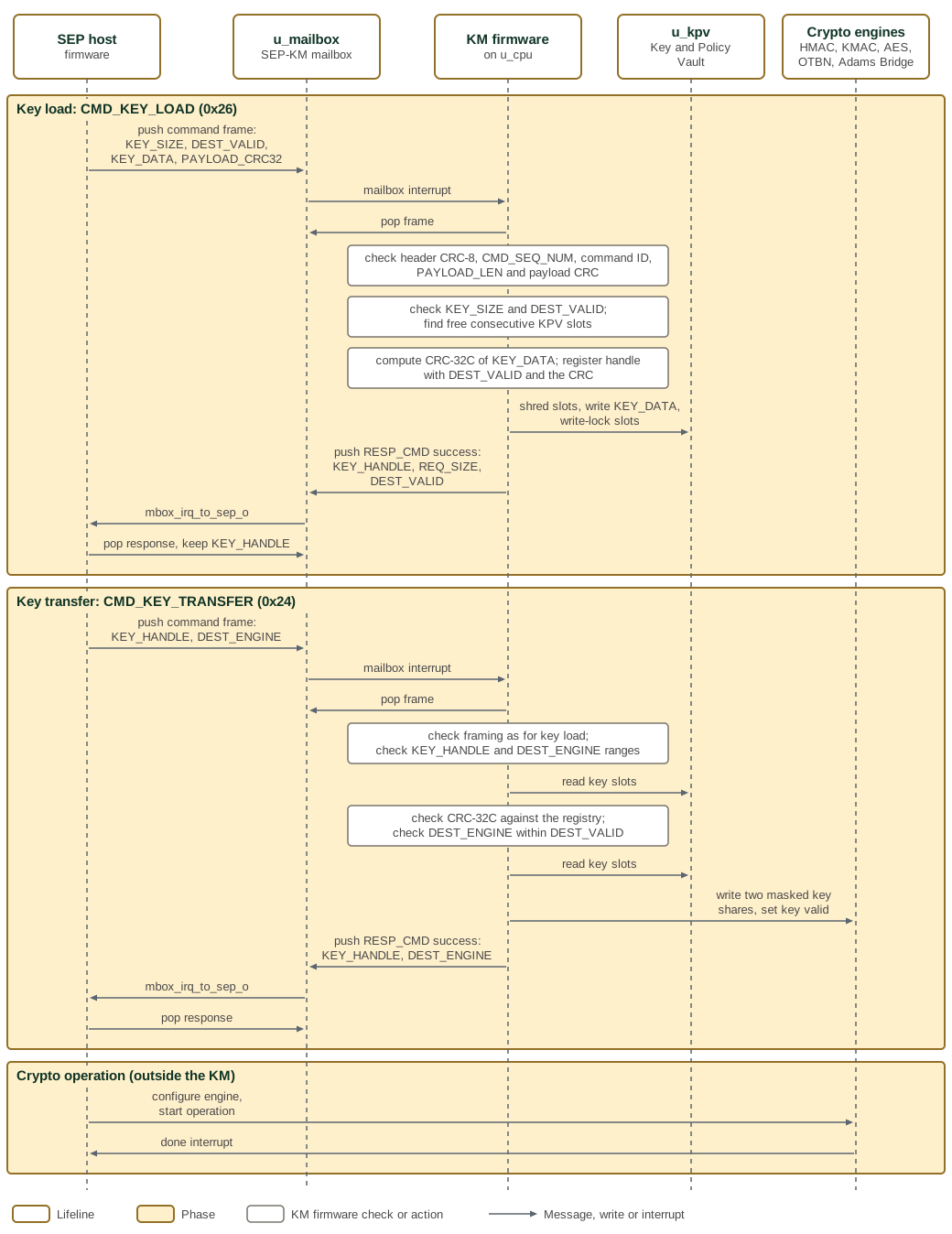
Time runs downwards. Each arrow is a mailbox word push or pop, a register write
or read, or an interrupt, and each white box is a check or action the KM
firmware performs without leaving the CPU. The figure shows the success path.
A failed check ends the command with a RESP_CMD error code and leaves the KPV
and the key registry unchanged.
On a key load, the firmware registers the handle before it writes the KPV, and
destroys the handle again if a KPV write fails. On a key transfer, the firmware
reads the key slots twice: once to check their CRC-32C against the key
registry, and again to write the key. Each requested engine receives the key as
two key shares whose XOR is the key, the first a DRBG mask, before its key-valid
bit is set. The engines are written in the order of their DEST_ENGINE bits,
and the first failed write ends the transfer.
1.8. Key and Policy Vault (KPV)
The KPV exposes 64 slots through one KM-only AXI4-Lite interface. Each slot
contains 512 bits (16 words) of key data and a 32-bit CTRL register.
Multi-slot keys, such as RSA3K material, require consecutive slots; the
firmware registry tracks the span and the used words in the final slot.
Hardware has no span field.
| Field | Behavior |
|---|---|
|
Write-one-to-set. Blocks key-data writes with SLVERR; does not block CTRL
writes or erase. Hardware holds it set while |
|
Write-one-to-set. Key-data reads return zero with SLVERR. Also set when an erase completes on a sealed slot. |
|
Write one to overwrite all 16 words with pseudorandom data. No lock blocks
erase. Poll until hardware clears the bit. If the slot is unsealed at
completion, all CTRL bits clear and the slot is reusable. If sealed at
completion, it is retired: |
|
Write-one-to-set. Implies a write lock. Erase destroys the contents without making the slot reusable; taking a seal during an erase also causes retirement. |
|
Reserved. |
The lock/seal bits clear on warm or cold reset. Erase uses the shared scrambler and key-data write port, so key-data accesses during an erase are not defined. The KPV driver in the Key Manager Application ROM appendix of the Programmer’s Guide gives the erase sequence.
Sealed and retired slots. A slot with seal set is sealed: readable, but not writable, because hardware holds lock_write set alongside the seal. That surviving lock_write is evidence that the slot holds what it held when the seal was taken, which is what lets firmware that inherits the vault after a handover trust material provisioned before it. A write lock on its own would prove nothing, since an erase clears it and frees the slot to be rewritten with chosen material and re-locked.
Erasing a sealed slot is still permitted, and leaves it retired: lock_write held, lock_use set, seal still set, and the data destroyed. A retired slot can be neither read, rewritten nor reused until the next warm reset, and repeating the erase changes nothing. Revocation and reuse are therefore separate: firmware can destroy a sealed key it no longer trusts without handing the slot to whoever asked for the destruction.
An emergency wipe also releases sealed and retired slots by clearing key data
and all CTRL bits. The safety of that release depends on CPU containment:
a trap already halts the CPU, whereas an externally requested wipe requires
firmware or host coordination (Section 1.10). Do not assume that asserting
wipe_state_i directly halts CPU execution.
CTRL resets to zero. Key-entry data flops have no reset value and power up undefined; cold or warm reset alone does not overwrite their contents.
1.9. KPV Scrambling
The KPV supports address and data scrambling during normal operation for all key entry data reads and writes, using the same PRESENT-based approach as SRAM scrambling. When enabled, the stored representation of key data is scrambled; the KM port sees the logical (unscrambled) data on the bus, with scrambling/descrambling performed transparently by the KPV.
The KPV has a scrambler key register (32-bit) and a scrambler control register with an enable bit and a lock bit. These registers are accessible only via the KM port. The lock bit is write-one-only (0→1): software sets lock by writing 1; writing 0 has no effect; lock cannot be cleared until the next cold KM reset. The KPV scrambler enable and lock are state in the cold reset domain — they are preserved across a warm reset and cleared only by a cold reset. Scrambling is disabled by default after a cold reset.
When scrambling is enabled, the KPV uses the same scrambler algorithm as
SRAM but sized for 1024×32 words (64 slots × 16 words). The scrambler
address input is the linear register index (0..1023): slot_index × 16
word_index. Address scrambling maps the logical index to a scrambled
physical storage index. Data is scrambled before storage and descrambled
after retrieval. Only key entry data words are scrambled; CTRL registers
are not scrambled.
The KPV scrambler key register has no reset value (powers up random/undefined for security). The scrambler control register (enable and lock) resets to 0. On an emergency wipe (rising edge of wipe_state), the entire KPV is reset to zero including key data, control registers, and the KPV scrambler key and control registers.
1.10. Wipe State
Hardware forms a wipe event from wipe_state_i | cpu_trap and detects its
rising edge. The resulting pulse clears all 1024 KPV data words, all 64 slot
CTRL registers, and KPV scrambler key/enable/lock state on the clock edge.
It also records the KMCSR wipe event. This hardware action covers the KPV;
it does not itself scrub SRAM, mailbox data or accelerator sideload registers.
In SEP, sep_cpu_ctrl.KM_WIPE_CTRL.wipe_state drives the external input.
Hold it high for at least one complete KM clock period. Return it to zero
before requesting another rising edge; the software-controlled registered
level provides the required hold. SEP does not connect a hardware tamper or
alarm source to this input. A CPU trap independently triggers the same KPV
wipe and asserts unrecoverable_err_o while the CPU is halted.
An external wipe does not force a CPU trap in hardware. The ROM enables the wipe interrupt and treats it as an unrecoverable fault, but that response depends on interrupt delivery and execution of its handler. Software that masks the event or replaces ROM must not assume the CPU has stopped. The host/integrator must prevent continued use of the released vault after an external wipe until recovery resets the CPU. Warm reset clears the trap and re-enters ROM; it is not itself the KPV data erase mechanism.
1.11. Scan and Scan-Dump Protection
The complete KM is Class 2 under SEP’s scan-chain protection policy: processor, vault, KMCSR, mailbox, entropy sampler, scramblers, internal fabric, reset logic and register blocks. Including non-secret control state avoids relying on a per-register classification.
-
Test scanning is permitted only in secure test mode. The dedicated-chain DFT controller admits test commands only with
secure_tm = 1. At the eFuse shadow boundary, this mode replaces the four Class 1 sources (*_UIDandCLASS_KEY) with valid zero values before KM captures them. Those source assets remain outside every scan chain. Public identities, lifecycle and demotion policy remain available. -
Scan dump is never permitted. No lifecycle state, owner or combination of
*_DBGfeature enables may turn a test command into a dump. Feature controls determine whether the chain is reachable; the command-class restriction enforces the no-dump policy. General-logic debug enablement does not grant access to the KM secret-bearing chain.
KM-local copies of the UIDs, class key and public identities clear on cold and warm reset (including firmware soft reset) and reload from the shadow bus after release. Lifecycle/demotion captures persist across warm reset. Firmware access locks are independent of scan protection.
Writable KM SRAM is a Class 2 companion memory because it can retain key, message and firmware working state. Its memory-test policy must also forbid dump. Immutable ROM cannot retain runtime secrets and is excluded. These requirements define the integration boundary; the local KM RTL alone does not establish implementation of the external DFT controller.
1.12. Key Manager Control and Status Registers (KMCSR)
KMCSR manages interrupts, reset requests, execution permissions, memory
protection and OTP shadow readout. It is separate from the KPV and DRBG
sampler banks. km_csr supplies the behavior around generated km_csr_reg;
Section 3.2.2 supplies every offset and field definition.
The operating contracts below supplement that generated map.
The VERSION register (offset 0x000) is a read-only register that reports
the Key Manager hardware revision using semantic versioning. It uses the
following canonical 32-bit layout, mandated so all software and testbenches
decode the version identically (Table 8).
| Bits | Field | Description |
|---|---|---|
|
|
Patch version component. |
|
|
Minor version component. |
|
|
Major version component. |
|
|
Reserved; reads as 0. |
The current hardware revision reads as version 1.0.0 (MAJOR=1, MINOR=0,
PATCH=0) after reset with no software initialization. The register is
read-only: a write completes with an AXI SLVERR response and does not change
the value.
The interrupt aggregation logic collects twelve hardware event sources into a
single CPU interrupt. Each source has a sticky status bit in IRQ_STATUS
(write-one-to-clear), a mask bit in IRQ_ENABLE, and a software-trigger bit in
IRQ_SET for ISR testing. The aggregated interrupt output is the logical OR of
the masked status bits (IRQ_STATUS & IRQ_ENABLE).
Table 9 maps hardware events to the sticky interrupt-status bits.
| Bit | Source | Description |
|---|---|---|
0 |
ROM Parity Error |
Parity mismatch detected on a ROM read. |
1 |
SRAM Parity Error |
Parity mismatch detected on an SRAM read. |
2 |
ROM Write Error |
A write was attempted to the read-only ROM region. |
3 |
SRAM Write-Lock Violation |
A write targeted a locked 1 KB SRAM region. |
4 |
AXI SLVERR |
An AXI4-Lite slave returned SLVERR. |
5 |
AXI DECERR |
An AXI4-Lite slave returned DECERR. |
6 |
DRBG Error |
The DRBG sampler reported a timeout or stream error. |
7 |
Wipe State |
Rising edge detected on the |
8 |
OTP Change |
A monitored OTP readout field’s decoded value changed (see |
9 |
OTP Integrity Violation |
OTP dual-rail integrity violation (value and complement not complementary). |
10 |
Execute Violation |
Instruction fetch from a non-whitelisted (non-executable) memory region, excluding the ROM. |
11 |
ROM Access Violation |
ROM instruction fetch or data read attempted after the ROM lockout engaged. |
Bits [31:12] of IRQ_STATUS are reserved. Two interrupt sources are not part
of the KMCSR IRQ_STATUS aggregation and are serviced separately: the mailbox
sources (FIFO data-available/space-available and overflow/underflow/flush
conditions), and the Adams Bridge ML-KEM shared-key interrupt on its own
PicoRV32 interrupt (bit 5, see Section 1.5).
The CPU IRQ entry vector is programmable through two registers. IRQ_ENTRY_ADDR
holds the effective IRQ entry address and resets to the built-in default
0x0000_0010; firmware may write any 32-bit value (the hardware performs no
alignment or validity checking) and the register is always readable, returning
the current effective entry address. IRQ_ENTRY_LOCK is a write-one-only lock
bit that can only transition from 0 to 1: while it is 0 firmware may reprogram
IRQ_ENTRY_ADDR freely; once it is 1, writes to IRQ_ENTRY_ADDR are ignored
(the value remains readable and unchanged) and further writes to
IRQ_ENTRY_LOCK have no effect. Both registers are in the warm reset domain:
every reset that re-enters ROM (cold, external warm, and KM soft reset)
restores IRQ_ENTRY_ADDR to 0x0000_0010 and clears IRQ_ENTRY_LOCK.
SRAM_LOCK controls writes to 32 SRAM regions of 1 KB each; see
Section 1.18 for reset and handover policy. SRAM scrambling
key/enable/lock state is cold-domain state and survives warm reset.
The soft-reset code and cold-boot flag are described under Reset Conditioning.
Execute-Permission Whitelist (NX)
The PicoRV32 enforces a whitelist of executable memory regions on every
committed instruction fetch (mem_valid && mem_instr). Any fetch from
outside the whitelist immediately pulses KMCSR.IRQ_STATUS.EXEC_VIOLATION,
which (if unmasked) routes to the ISR and triggers the unrecoverable fault
ROM_KM_UFAULT_EXEC. A ROM fetch refused by the ROM lockout described below
is reported on ROM_ACCESS_VIOLATION instead, so the two bits are disjoint.
The whitelist mode is controlled by the KMCSR.SRAM_EXEC_MODE.enable bit
(write-1-only, warm-reset domain) (Table 10).
enable |
Executable regions | Forbidden regions |
|---|---|---|
|
ROM ( |
All SRAM; Peripheral/AXI |
|
Write-locked 1 KB SRAM regions ( |
Unlocked SRAM; Peripheral/AXI; the ROM once the lockout engages |
The fetch-region index is a plain slice of the byte address, which works only
because the SRAM base (0x0000_8000) is aligned to the SRAM size; it is the
same slice km_sram_interface uses to check data writes, so the two views of a
region can never disagree.
-
VROM is the virtual ROM window,
0x1000_0000–0x1000_FFFF. Only a simulation build that definesOCAH_KM_VROMdecodes it; there it is executable in both modes and exempt from the ROM lockout, and it carries no security requirement. Without the define the window is an unmapped address: a load or store answers DECERR, and a fetch pulsesEXEC_VIOLATION.
For the define and the builds it is rejected in, see Key manager defines in the Integrator Guide.
SRAM_EXEC_MODE.enable is set by the stack-less handover assembly
(rom_handover_jump.S) immediately before the jalr to mutable firmware,
after SRAM write-lock regions have already been committed. This minimises
the window between enabling SRAM execution and the first fetch from SRAM.
The bit is write-1-only and cleared by warm reset, so the ROM-only
whitelist is re-applied on every boot cycle.
ROM Lockout
Setting SRAM_EXEC_MODE.enable exchanges the ROM for write-locked SRAM rather
than adding to the whitelist. Were it purely additive, mutable firmware would
inherit read and fetch access to the ROM that handed control to it, leaving the
ROM’s key-management routines and its rom_persist structure reachable by code
the ROM does not trust.
The exchange is staged so that the handover can complete. Writing the bit only
arms the lockout; the lockout engages on the first committed instruction
fetch from a write-locked SRAM address, which is the point at which mutable
firmware actually begins executing. Everything the handover assembly runs after
its arming store — the store itself, the register clears, the jalr — is ROM
code, and remains legal precisely because the lockout has not engaged yet.
Engaging on a fetch rather than on any ROM access also keeps the rule
independent of incidental data traffic: ROM code reads rom_persist, which
itself lives in a write-locked SRAM region.
Once engaged, the lockout blocks ROM instruction fetches and ROM data reads
until the next warm or cold reset. The latch is in the warm reset domain, the
same domain as SRAM_EXEC_MODE.enable, so the transition is one-way within a
boot and every reset that re-enters ROM restores ROM access. ROM writes are
unaffected and continue to raise ROM_WRITE_ERR.
Blocked access behaviour. A blocked access returns zeros; ROM content is never delivered. What follows depends on the access type:
-
A blocked data read raises
ROM_ACCESS_VIOLATIONand nothing else. Zero is a legitimate data value, so no decode and no trap occur. -
A blocked instruction fetch raises
ROM_ACCESS_VIOLATIONand additionally feeds an all-zeros instruction stream, which the PicoRV32CATCH_ILLINSNlogic traps as an illegal instruction.
The two reports are ordered by causality rather than by arbitration. The
violation is combinational in the cycle of the blocked access, whereas the
illegal instruction cannot be detected until the zero word has been returned and
decoded, which is strictly later. Since IRQ_STATUS is sticky, the violation
bit is always recorded first.
Which mechanism acts depends on the interrupt mask, and after handover only
one does. Handover leaves all CPU interrupts masked, so the illegal instruction
takes the PicoRV32 trap state rather than an interrupt: the core halts,
unrecoverable_err_o asserts, and the KPV is wiped. The ROM_ACCESS_VIOLATION
interrupt is inert in that state — it sets its sticky bit but has nowhere to
vector, because the ROM ISR it would have vectored to is itself in the ROM the
lockout has just revoked. A real post-handover breach therefore halts the KM
without emitting a mailbox fault code; ROM_KM_UFAULT_ROM_ACCESS is reportable
only while the ROM is still live (via IRQ_SET) or through a vector that
mutable firmware installed itself.
Both mechanisms are retained because they do different jobs. The violation bit is the diagnostic that distinguishes a lockout breach from any other illegal-instruction halt; the trap is the containment, and it requires no firmware cooperation, no enabled interrupt, and no reachable handler.
Error Events
Unrecoverable Faults
These events cause the CPU to halt when the corresponding interrupt is unmasked and the ISR determines recovery is not possible. They include, but are not limited to, the following conditions:
-
CPU trap events
-
ROM or SRAM parity errors
-
Invalid writes to ROM or SRAM
-
AXI bus faults (SLVERR or DECERR)
-
Instruction fetch from a non-whitelisted (non-executable) memory region
-
ROM instruction fetch or data read after the ROM lockout engaged
-
Any other unhandled exception or fault
The PicoRV32 includes a trap state that asserts a trap signal. When the CPU enters this state execution halts. The CPU will enter this state under the following conditions:
-
An EBREAK or other illegal instruction is encountered and the associated interrupt is masked.
-
The CPU encounters a misaligned access and the associated interrupt is masked.
-
An EBREAK or other illegal instruction is encountered within an ISR.
If an ISR determines that an error event is not recoverable, it will call the EBREAK instruction to trap and halt the core. The CPU trap signal is passed out of KM to indicate an unrecoverable fault. This signal indicates the KM has encountered an unrecoverable fault and is no longer executing (it will not respond to further commands). The signal remains asserted for as long as the KM remains in the trap state. The trap is cleared by resetting the KM CPU — either a cold reset or a warm reset (the PicoRV32 core is in the warm reset domain) restarts the core and clears this signal.
Recoverable Faults
These events do not cause the CPU to halt. They include:
-
Receiving corrupt or malformed command messages.
-
Detection of possible tampering or attack conditions that are not immediately terminal.
-
Any one of the previously listed error interrupts from which the corresponding ISR is able to gracefully recover.
The KM provides an output signal that indicates when a recoverable fault has been successfully handled. This signal is driven by a dedicated register bit in the KMCSR. When an ISR recovers gracefully from an error, it sets this register bit. The bit remains set until the SEP sends a firmware command to the KM to clear it (KM firmware clears the register bit in response to that command).
1.13. DRBG Sampler
The sampler bridges a CPU DATA read to the selected 32-bit entropy stream.
It is an AXI4-Stream sink: TREADY is an output, and TVALID, TDATA[31:0]
and TSTRB[3:0] are inputs. Availability is not guaranteed; a pending read
waits for a word or an enabled timeout.
1.13.1. Reads, prefetch and register access
A DATA read consumes a prefetched word if one is available. Otherwise the
sampler asserts TREADY and assembles four valid bytes before completing the
AXI read. TSTRB selects bytes to pack in beat order, walking lanes 0 through
3; partial beats require further handshakes. Bytes beyond the four needed
for the current word are not carried into the next word.
CFG.PREFETCH enables a single prefetched word. Consuming it through DATA
invalidates it; prefetch alone does not increment the direct-read success
counter. Disabling prefetch clears its data/valid state. The read-only
PREFETCH_DATA register exposes the stored word for debugging and does not
consume it, so repeated debug reads are not fresh random samples.
| Register or field | Access and meaning |
|---|---|
|
Read obtains a sample; writes return SLVERR. |
|
Read/write; reset 0 (disabled). |
|
Read/write active-read wait budget in clocks; reset 256. The counter loads |
|
Read-only indication of input |
|
Read-only indication that a prefetched word is available. |
|
Sticky timeout indication; write one to clear. |
|
Sticky stream-protocol error; write one to clear. |
|
Timeout/stream-error count, saturating at |
|
Counts only reads completed through |
|
Read-only debug view; writes return SLVERR. |
Because prefetched reads bypass ST_RESPOND, COUNT_GOOD is not a total of
all DATA reads when prefetch is enabled.
1.13.2. Errors and reset
Timeout completes an active read with SLVERR and zero data. The protocol
monitor detects a different event: previous-cycle TVALID=1, TREADY=0,
followed by TVALID=0 (withdrawal before handshake). It sets STREAM_ERR,
increments COUNT_BAD and pulses the KMCSR DRBG error source even when no
read is active. If the active FSM is requesting or assembling a word, it
also returns SLVERR with zero data. A prefetch in progress is discarded.
A TVALID drop after a completed handshake is not this violation.
The sampler is in the KM warm-reset domain, not the TRNG reset domain. Quiesce KM before resetting the TRNG. Resetting the producer alone can withdraw an unaccepted beat or interrupt byte assembly; it does not clear partial bytes held by the sampler. Holding KM in software reset clears sampler control/assembly state before the source restarts.
Warm or cold KM reset restores configuration defaults, counters, error bits, valid flags and request/assembly control. Data registers (prefetch data, assembly storage and the response slot) have no reset value; invalidating their control state is not a guaranteed data scrub.
| State | Active DATA-read behavior |
|---|---|
|
Returns an available prefetch without entering |
|
Asserts |
|
Keeps |
|
Completes the assembled read with OKAY and increments |
|
Completes with SLVERR and zero data after the active wait budget expires; returns to idle. |
|
Completes with SLVERR and zero data after a detected withdrawal during request/assembly; returns to idle. |
A separate prefetch FSM uses the request/assembly states. It accepts beats
only when there is no active CPU DATA read. In the active request/assembly
states, a stream error takes priority over timeout, and timeout takes
priority over accepting a completing beat.
1.14. OTP Inputs and Readout
The KM consumes OTP-derived material over a private hardwired bundle so the
values cannot be spoofed by software. SEP dual-rail-encodes each 256-bit field
at the SEP-to-KM boundary ({~value, value}) from the sensed eFuse shadow:
-
the fuse-provisioned secrets —
CHIPLET_UID,SIP_UID,SYS_UID,CLASS_KEY; -
the three 256-bit public identities —
SEP_CHIPLET_ID,SEP_SIP_ID,SEP_SYS_ID— one per owner; -
the life-cycle state.
UID delivery and protection. The UIDs are held in a KM-local copy. The KM’s own warm-domain read-lock protects that copy at mutable-firmware handover (see UID provisioning and access) so mutable firmware cannot read it. This KM-local lock is separate from, and additional to, the eFuse controller’s own locks.
Public identity delivery. The three public identity fuses take the same
dual-rail encode as the secrets. They remain on the KM port in secure test
mode: the eFuse controller blanks only the four secrets on the hardware shadow
output. The eFuse per-field read-lock bits (LOCKS[59], [61], [63]) hide
software and JTAG shadow reads; they do not blank the hardwired KM port. The
KM’s own OTP_READ_LOCK and OTP_READ_LOCK_COLD bits zero the KMCSR readout
words only.
Life-cycle state. The life-cycle state is hardwired into the KM as authoritative, software-readable status. Being non-secret it is neither locked nor wiped. The key registry does not bind keys to it.
eFuse access path. The KM also has a programmatic (AXI-Lite) path to the eFuse controller — for example to request a read or a program operation. That path is treated exactly like a system-host access: same access filtering, and it honors the eFuse controller’s native per-field read/write locks, so the KM gains no read privilege over the fuse array beyond the SEP host’s.
Demotion and PCR. The owner demotion state is hardwired from the Life Cycle Controller (LCC). A PCR Vault (PCRV) and PCR-change interrupt are not present in this integration.
KMCSR readout registers. The OTP-derived fields above are exposed to KM
firmware in the KMCSR region as hardware-driven, read-only registers. Each field
is delivered to the KMCSR as dual-rail complementary values ({~value, value})
and decoded within the KMCSR, which continuously verifies the complement
relationship.
Table 13 lists the OTP-derived fields exposed to Key Manager firmware.
| Register | Width | Contents |
|---|---|---|
|
8-bit |
Differential-encoded life-cycle state |
|
4-bit |
Two 1-bit demotion flags, each differentially encoded into 2 bits: |
|
8 × 32-bit |
256-bit CHIPLET_UID dual-rail words. |
|
8 × 32-bit |
256-bit SIP_UID dual-rail words. |
|
8 × 32-bit |
256-bit SYS_UID dual-rail words. |
|
8 × 32-bit |
256-bit CLASS_KEY dual-rail words. |
|
8 × 32-bit |
256-bit SEP_CHIPLET_ID dual-rail words. |
|
8 × 32-bit |
256-bit SEP_SIP_ID dual-rail words. |
|
8 × 32-bit |
256-bit SEP_SYS_ID dual-rail words. |
|
9-bit |
Write-one-to-set read-lock bits (warm reset domain), one per field. Cleared by warm or cold reset. |
|
9-bit |
Write-one-to-set read-lock bits (cold reset domain), one per field. Survives warm reset; cleared only by cold reset. Effective lock = |
|
9-bit |
Sticky write-1-to-clear flags: set when a monitored field’s decoded value changes. |
Dual-rail integrity. The hardware continuously checks that each value word is
the bitwise inverse of its complement word. Any violation raises the
OTP_SIGINT interrupt, which ROM firmware treats as an unrecoverable fault.
This applies to the public identity fields as much as to the secrets.
Change detection. When a monitored field’s decoded value changes, the hardware
sets the corresponding OTP_CHANGE_STATUS bit and raises the OTP_CHANGE
interrupt. ROM firmware reads the status, invokes an overridable change hook, and
clears the flag. Spurious change events are suppressed until the capture history is valid
after cold or warm reset.
Unique Identifiers (UID) — provisioning and access
The KM receives three fuse-provisioned Unique Identifiers — CHIPLET_UID,
SIP_UID, and SYS_UID (256 bits each) — provisioned respectively by the
chiplet creator, the SiP owner, and the system owner. ROM does not derive keys
from them.
The CPU services mailbox commands from ROM and supports loading and executing SRAM firmware. Before handing control to that firmware, ROM applies the OTP read locks and wipes secrets from the shared execution environment. A warm reset returns the CPU to ROM, where the handover protections are re-established.
Concretely, this safeguard is the OTP_READ_LOCK register: one
write-one-to-set bit per OTP readout field (life-cycle, demotion, the four
256-bit secrets, and the three 256-bit public identities). Setting a bit causes
the hardware to return zero for that field’s value and complement words. ROM
applies the lock using a triple-write convention (three consecutive writes) so
it commits even under a single-bit glitch. OTP_CHANGE_STATUS shares the same
warm reset domain for the same reasons.
ROM does not lock the public identity fields at handover, since concealing them buys nothing. Their lock bits suppress KMCSR readback like those of the secret fields.
A parallel cold-reset-domain register, OTP_READ_LOCK_COLD, provides the
same write-one-to-set, per-field locking semantics but survives warm reset
(including soft reset) and is cleared only by cold reset. The effective
read-lock for each field is the OR of the corresponding bits in OTP_READ_LOCK
and OTP_READ_LOCK_COLD; either register alone is sufficient to suppress CSR
readback. The SEP host can set cold-domain lock bits at any time by issuing
CMD_OTP_READ_LOCK_COLD (0x28) over the KM mailbox. This allows the SEP host
to establish read-locks that persist across warm resets for the entire duration
of a power cycle, independently of the warm-reset lock applied by ROM firmware.
1.15. CRC Accelerator
The KM CPU is fitted with a CRC accelerator attached through the PicoRV32 PCPI (Pico Co-Processor Interface). It provides hardware versions of the CRC functions the firmware uses on its high-value integrity paths — message header CRC-8/ROHC, message payload CRC-32C, and key-data integrity CRC-32C — so these computations consume far less CPU time than a software loop. The accelerator is always present in the KM build; firmware invokes it unconditionally and does not retain a software fallback path.
The accelerator exposes three R-type custom instructions on the PicoRV32
custom0 opcode. Each instruction takes two operands — the current CRC
chaining state (rs1) and the next input unit (rs2) — and writes the
updated chaining state to rd.
Table 14 lists the instruction encodings and input units for the hardware CRC updates.
| Instruction | funct7 |
funct3 |
opcode | Input unit |
|---|---|---|---|---|
CRC-32C word update |
|
|
|
|
CRC-32C byte update |
|
|
|
|
CRC-8/ROHC byte update |
|
|
|
|
Behavioral properties:
-
The CRC-32C word-update instruction consumes its 32-bit operand as four bytes in little-endian order (
[7:0],[15:8],[23:16],[31:24]). -
The CRC-32C instructions expose the internal running remainder before the final XOR. Firmware seeds the chaining state with
0xFFFF_FFFFand applies the final XOR only when it needs the externally visible CRC value, so word updates, byte updates, and intermediate states chain freely. -
For non-word-sized buffers, firmware processes whole words with the word-update instruction and any remaining
1–3tail bytes with the byte-update instruction; no software tail path is used. -
The CRC-8/ROHC instruction carries its 8-bit state in
rd[7:0]and zero-extendsrd[31:8]. -
Empty-input results are identical to the software definitions: with no input units consumed, the seeded state (after the firmware’s final XOR for CRC-32C) is the empty-input CRC.
The three instructions share a single byte-update datapath. CRC-32C word
mode runs four byte-update cycles per operation; the two byte modes run
one cycle each. The datapath uses reflected CRC update behavior with the
reflected polynomial 0x82F6_3B78 for CRC-32C and 0x0000_00E0 for
CRC-8/ROHC (the reflection of the 0x07 CRC-8/ROHC polynomial), and never
applies the CRC-32C final XOR. The CRC parameter definitions (init,
reflection, and final XOR) are given in the firmware CRC function library
documentation.
Any other encoding in the custom0 CRC instruction family is not
recognized by the accelerator: it does not assert the PCPI ready/wait/write
handshakes, so PicoRV32’s normal illegal-instruction handling is
preserved. The feature introduces no new top-level KM ports or CSRs, and
the PicoRV32 built-in multiply/divide support remains enabled and
unchanged.
1.16. ROM and SRAM Error Detection
ROM and SRAM use one odd-parity bit per byte: four parity bits accompany each 32-bit data word. Checking cannot be disabled and performs no correction. Interrupt enables control reporting to the CPU; masking an event does not repair the affected data or make it safe to use.
1.17. Parity Error Protection
Parity bits are stored out-of-band, outside the scrambled data word. This keeps parity storage separate from the scramble/descramble data path.
1.18. SRAM Write Locking
The SRAM interface incorporates a write-locking mechanism to designate
specific 1 KB memory regions as read-only; 32 regions cover the whole 32 KB
SRAM, one per SRAM_LOCK bit. This feature is primarily
designed to protect dynamically loaded KM firmware from unauthorized
modification.
Control of this functionality resides within the Key Manager Control and Status Registers (KMCSR). Once a memory region is locked, it cannot be unlocked within the current boot session. It will remain in the read-only state until the next warm or cold reset of the KM. The write-lock state is in the warm reset domain and is cleared on every warm or cold reset.
Protection across warm resets is maintained by the ROM, which is responsible for re-applying the full write-lock policy on every boot (both cold and warm) before handing control to mutable firmware. Because the KM CPU always re-enters ROM after a warm reset, mutable firmware never executes against an unlocked SRAM region.
1.19. ROM Warm-Persistent SRAM Region
The highest 1 KB of KM SRAM (region 31, 0x0000_FC00–0x0000_FFFF) are
reserved as a ROM-managed warm-persistent data structure (rom_persist). The
mutable-firmware load area, stack, and BSS/data occupy the SRAM below it.
This region is owned exclusively by ROM firmware: it holds ROM state that must survive warm reset and is not general-purpose scratch for mutable (SRAM-loaded) firmware. Mutable firmware must not place its own data here, and once ROM write-locks the region it cannot write it at all (see Write-lock policy below).
SRAM contents survive warm or soft reset. Reset of the memory interface does not itself specify an array erase. ROM carries state across warm resets and initializes this structure on cold boot; this is volatile SRAM retention, not non-volatile storage.
Cold initialization. On every cold boot, rom_boot_init() detects a cold
boot via the COLD_BOOT_DONE flag (reads 0 before it is set at the end of
boot) and calls rom_persist_cold_init(), which writes known-zero values to
all fields. On a warm or soft reset, COLD_BOOT_DONE already reads 1 and
rom_persist_cold_init() is skipped, preserving the contents of the region.
Contents. The rom_persist_t structure currently contains one field (Table 15).
| Field | Type | Description |
|---|---|---|
|
|
Byte count of the mutable firmware image currently loaded in SRAM ( |
Write-lock policy. Before handing control to mutable (SRAM-loaded) firmware,
ROM must call rom_persist_lock(), which sets SRAM_LOCK bit 31 via a triple
write for glitch resistance. After locking, any write into 0xFC00–0xFFFF
is silently dropped and a SRAM_WRITE_LOCK_VIOLATION IRQ is raised. The lock
is cleared on the next warm or cold reset; ROM re-establishes it
before transferring control to mutable code.
1.20. Mutable Firmware Model
The KM ROM can load a mutable image into SRAM and hand control to it, through
the CMD_SRAM_LOAD_EXEC and CMD_SRAM_EXEC mailbox commands. The image is
loaded at 0x8000, which is also its entry point, and must fit below a static
load ceiling aligned to a 1 KB write-lock region, so the image never shares a
region with the ROM stack or data. The load bounds, the key shred, the KPV
read-lock, the image write-lock, the mailbox flush, the SRAM scramble and the
jump are ROM behaviour, defined in the
SRAM Firmware Handover
sequence of the Key Manager Application ROM appendix in the Programmer’s
Guide.
The handover relies on the following hardware behaviour:
-
SRAM_LOCKis in the warm-reset domain. A warm reset clears the image write-lock, and ROM re-applies it before every handover, including aCMD_SRAM_EXECrestart. -
IRQ_ENTRY_ADDRandIRQ_ENTRY_LOCKare warm-reset-domain registers. Every reset that re-enters ROM (cold, external warm, and KM soft reset) restores the vector to the ROM default (0x10) and clears the lock, so ROM never executes with a vector chosen by mutable firmware. -
KPV key data has no warm reset and is descrambled on KM-port reads.
lock_useis independent oflock_writeand makes KM-port key reads return zero. -
The crypto-engine sideload key registers lie outside the SRAM address space, so scrambling SRAM does not reach them.
-
Writes to a write-locked SRAM region are dropped and raise
SRAM_WRITE_LOCK_VIOLATION, which is sticky until cleared.
2. Firmware
The KM ROM and any mutable firmware it hands over to run on the PicoRV32. The Key Manager Application ROM appendix of the Programmer’s Guide is the firmware reference: initialization, the mailbox command and response protocol, interrupt handling, key management and the SRAM handover rules.
3. Memory Map and Register Reference
3.1. Memory Map
The KM CPU addresses its internal peripherals through a flat 32-bit address space. The AXI4-Lite crossbar decodes the address and routes transactions to the corresponding slave port.
Every window except OTP/eFuse spans exactly the address bits its register block decodes, so no register is reachable from a second address. The last two columns of the map state how the crossbar and the register blocks answer an access that no register or memory backs, and
Decode Response Codes
defines them and their codes. The KM CPU does not see these responses: an error sets AXI_SLVERR or AXI_DECERR in the KMCSR IRQ_STATUS register.
The OTP/eFuse window is the exception: hardware preserves its lower 12 address
bits and replaces the upper bits with the integration parameter
OTP_EFUSE_REMAP_BASE before forwarding the transaction to SEP. Only the
MAP, CTRL and MMR register maps are forwarded. The Key Manager answers any
other offset in the window with SLVERR, so the KM CPU cannot reach the eFuse
shim control registers.
| Base Address | End Address | Size | Decoded Extent | Unit | Description | Hole in Extent (R / W) | Past Extent (R / W) |
|---|---|---|---|---|---|---|---|
0x00000000 |
0x00003FFF |
16 KiB |
16 KiB |
Key Manager ROM |
Key Manager boot ROM |
-[1] |
- |
0x00004000 |
0x00007FFF |
16 KiB |
16 KiB |
Reserved |
Reserved |
DECERR, 0xBADCAB1E / DECERR |
- |
0x00008000 |
0x0000FFFF |
32 KiB |
32 KiB |
Key Manager SRAM |
Key Manager data and executable SRAM |
- |
- |
0x00010000 |
0x0001001F |
32 B |
28 B |
Key Manager Mailbox KM Side |
Register interface for KM CPU to access mailbox (write to outbound FIFO, read from inbound FIFO) |
- |
SLVERR, 0x0 / SLVERR |
0x00010020 |
0x00010FFF |
4064 B |
4064 B |
Reserved |
Reserved |
DECERR, 0xBADCAB1E / DECERR |
- |
0x00011000 |
0x000113FF |
1 KiB |
1 KiB |
SEP eFuse Map Address Map |
SEP eFuse shadow-register pass-through. |
Forwarded |
- |
0x00011400 |
0x000114FF |
256 B |
28 B |
eFuse Interface Control Address Map |
SEP eFuse command and status pass-through. |
Forwarded |
SLVERR, 0xBADCAB1E / SLVERR |
0x00011500 |
0x000115FF |
256 B |
116 B |
eFuse Token Registers Address Map |
SEP eFuse security-token pass-through. |
Forwarded |
SLVERR, 0xBADCAB1E / SLVERR |
0x00011600 |
0x00011FFF |
2560 B |
2560 B |
Reserved |
Reserved |
DECERR, 0xBADCAB1E / DECERR[2] |
- |
0x00012000 |
0x00013FFF |
8 KiB |
4360 B |
Key and Policy Vault (KM Port) |
Key entry storage and KM control registers. Access conditioned by lock_write/lock_use. |
- |
SLVERR, 0x0 / SLVERR |
0x00014000 |
0x000147FF |
2 KiB |
1216 B |
Key Manager Control and Status Registers |
Control and status registers for the Key Manager subsystem |
SLVERR, 0x0 / SLVERR |
SLVERR, 0x0 / SLVERR |
0x00014800 |
0x00014FFF |
2 KiB |
2 KiB |
Reserved |
Reserved |
DECERR, 0xBADCAB1E / DECERR |
- |
0x00015000 |
0x0001500F |
16 B |
16 B |
DRBG Sampler |
DRBG random data interface and configuration/status registers |
- |
- |
0x00015010 |
0x00017FFF |
12272 B |
12272 B |
Reserved |
Reserved |
DECERR, 0xBADCAB1E / DECERR |
- |
0x00018000 |
0x0001807F |
128 B |
100 B |
OTBN Wrapper Key Registers |
Key storage registers for the OTBN sideload interface. Written by Key Manager CPU, drives keymgr_key_i on the OT OTBN core. |
- |
SLVERR, 0x0 / SLVERR |
0x00018080 |
0x00018FFF |
3968 B |
3968 B |
Reserved |
Reserved |
DECERR, 0xBADCAB1E / DECERR |
- |
0x00019000 |
0x0001907F |
128 B |
68 B |
AES Wrapper Key Registers |
Key storage registers for the AES sideload interface. Written by Key Manager CPU, drives keymgr_key_i on the OT AES core. |
- |
SLVERR, 0x0 / SLVERR |
0x00019080 |
0x00019FFF |
3968 B |
3968 B |
Reserved |
Reserved |
DECERR, 0xBADCAB1E / DECERR |
- |
0x0001A000 |
0x0001A07F |
128 B |
68 B |
KMAC Wrapper Key Registers |
Key storage registers for the KMAC sideload interface. Written by Key Manager CPU, drives keymgr_key_i on the OT KMAC core. |
- |
SLVERR, 0x0 / SLVERR |
0x0001A080 |
0x0001AFFF |
3968 B |
3968 B |
Reserved |
Reserved |
DECERR, 0xBADCAB1E / DECERR |
- |
0x0001B000 |
0x0001B07F |
128 B |
68 B |
HMAC Wrapper Key Registers |
Key storage registers for the HMAC sideload interface. Written by Key Manager CPU, drives keymgr_key_i on the OT HMAC core. |
- |
SLVERR, 0x0 / SLVERR |
0x0001B080 |
0x0001BFFF |
3968 B |
3968 B |
Reserved |
Reserved |
DECERR, 0xBADCAB1E / DECERR |
- |
0x0001C000 |
0x0001C7FF |
2 KiB |
1068 B |
Adams Bridge Key Sideload Registers |
Single AXI4-Lite window for all KM sideload interfaces to Adams Bridge. Contains four dual-share secret-seed inputs and one shared-key output. |
SLVERR, 0x0 / SLVERR |
SLVERR, 0x0 / SLVERR |
0x0001C800 |
0x0001CFFF |
2 KiB |
2 KiB |
Reserved |
Reserved |
DECERR, 0xBADCAB1E / DECERR |
- |
3.2. Detailed Register Map
3.2.1. Address Summary Registers
Key Manager Top-Level Address Map
Complete memory map for the Key Manager subsystem, including ROM, SRAM,
control/status registers, mailbox, and external crypto engine ports.
This address map is from the perspective of the KM CPU (PicoRV32).
Register Arrays:
- RMA_SIP_TOKEN_I[8]: 8 registers, base 0x11500, stride 0x4
- RMA_CHIPLET_TOKEN_I[8]: 8 registers, base 0x11520, stride 0x4
- SEC_DISABLE_TOKEN_I[8]: 8 registers, base 0x11540, stride 0x4
- KEY_ENTRY[64].WORD[16]: 1024 registers, base 0x12000 (KEY_ENTRY x64 stride 0x40, WORD x16 stride 0x4)
- CTRL[64]: 64 registers, base 0x13000, stride 0x4
- KEY_SHARE0[12]: 12 registers, base 0x18000, stride 0x4
- KEY_SHARE1[12]: 12 registers, base 0x18030, stride 0x4
- aes_wrapper_key.KEY_SHARE0[8]: 8 registers, base 0x19000, stride 0x4
- aes_wrapper_key.KEY_SHARE1[8]: 8 registers, base 0x19020, stride 0x4
- kmac_wrapper_key.KEY_SHARE0[8]: 8 registers, base 0x1A000, stride 0x4
- kmac_wrapper_key.KEY_SHARE1[8]: 8 registers, base 0x1A020, stride 0x4
- hmac_wrapper_key.KEY_SHARE0[8]: 8 registers, base 0x1B000, stride 0x4
- hmac_wrapper_key.KEY_SHARE1[8]: 8 registers, base 0x1B020, stride 0x4
- abr_wrapper_key.MLDSA_SEED.KEY_SHARE0[8]: 8 registers, base 0x1C000, stride 0x4
- abr_wrapper_key.MLDSA_SEED.KEY_SHARE1[8]: 8 registers, base 0x1C020, stride 0x4
- abr_wrapper_key.MLKEM_SEED_D.KEY_SHARE0[8]: 8 registers, base 0x1C100, stride 0x4
- abr_wrapper_key.MLKEM_SEED_D.KEY_SHARE1[8]: 8 registers, base 0x1C120, stride 0x4
- abr_wrapper_key.MLKEM_SEED_Z.KEY_SHARE0[8]: 8 registers, base 0x1C200, stride 0x4
- abr_wrapper_key.MLKEM_SEED_Z.KEY_SHARE1[8]: 8 registers, base 0x1C220, stride 0x4
- abr_wrapper_key.MLKEM_MSG.KEY_SHARE0[8]: 8 registers, base 0x1C300, stride 0x4
- abr_wrapper_key.MLKEM_MSG.KEY_SHARE1[8]: 8 registers, base 0x1C320, stride 0x4
- KEY[8]: 8 registers, base 0x1C400, stride 0x4
Register List:
| Address | Name | Access | Description |
|---|---|---|---|
| 0x10000 | KM_WRITE_DATA | W | Write data to outbound FIFO (KM→SEP messages) |
| 0x10004 | KM_WRITE_SEPARATOR | RW | Write 1 to set message separator on next outbound (KM→SEP) write. Cleared by hardware when that write completes. |
| 0x10008 | KM_READ_DATA | R | Read data from inbound FIFO (SEP→KM messages) |
| 0x1000C | KM_STATUS | RW | FIFO status information |
| 0x10010 | KM_IRQ_STATUS | RW | Interrupt status register |
| 0x10014 | KM_IRQ_ENABLE | RW | Interrupt enable register for KM CPU |
| 0x10018 | KM_CTRL | RW | Control register for mailbox behavior configuration |
| 0x11000 | LOCKS | RW | - |
| 0x11008 | LOCKS_SPARE | RW | - |
| 0x1100C | LC_STATE | R | - |
| 0x11010 | SBOOT_DIS | R | - |
| 0x11014 | TRANSIENT_RMA_EN | R | - |
| 0x11018 | SIP_DIS | RW | An owner's feature control vector. When set (1'b1), the corresponding feature is disabled. Layout: see the Disable Vector Format section of lifecycle_controller.adoc. |
| 0x11020 | SYS_DIS | RW | An owner's feature control vector. When set (1'b1), the corresponding feature is disabled. Layout: see the Disable Vector Format section of lifecycle_controller.adoc. |
| 0x11028 | RMA_SIP_TOKEN_DIGEST | R | - |
| 0x11048 | RMA_CHIPLET_TOKEN_DIGEST | R | - |
| 0x11068 | CLASS_KEY | R | - |
| 0x11088 | CHIPLET_PUBK_REVOKE | R | - |
| 0x1108C | BL1_VERSION | R | - |
| 0x110AC | BL2_VERSION | R | - |
| 0x110CC | CHIPLET_UID | R | - |
| 0x110EC | SIP_PUBK_HASH0 | R | - |
| 0x1110C | SIP_UID | R | - |
| 0x1112C | SYS_PUBK_HASH | R | - |
| 0x1114C | SYS_UID | R | - |
| 0x1116C | STATUS_RPT | R | - |
| 0x11170 | ROM_CTL | R | - |
| 0x11174 | SYSCLK_FREQ_MHZ | R | - |
| 0x11178 | CHIPLET_PUBK_HASH0 | R | - |
| 0x11198 | CHIPLET_PUBK_HASH1 | R | - |
| 0x111B8 | REQUIRED_SIGNERS | RW | - |
| 0x111BC | REQUIRED_ALGS | RW | - |
| 0x111C0 | CHIPLET_PUBK_PQC_HASH0 | R | - |
| 0x111E0 | CHIPLET_PUBK_PQC_HASH1 | R | - |
| 0x11200 | SIP_PUBK_PQC_HASH0 | R | - |
| 0x11220 | SYS_PUBK_PQC_HASH | R | - |
| 0x11240 | SIP_PUBK_HASH1 | R | - |
| 0x11260 | SIP_PUBK_PQC_HASH1 | R | - |
| 0x11280 | SEP_CHIPLET_ID | R | - |
| 0x112A0 | SEP_SIP_ID | R | - |
| 0x112C0 | SEP_SYS_ID | R | - |
| 0x112E0 | spare0 | R | - |
| 0x11300 | spare1 | R | - |
| 0x11320 | spare2 | R | - |
| 0x11340 | spare3 | R | - |
| 0x11360 | spare4 | R | - |
| 0x11380 | spare5 | R | - |
| 0x113A0 | spare6 | R | - |
| 0x113C0 | spare7 | R | - |
| 0x113E0 | spare8 | R | - |
| 0x11400 | EFUSE_INTERFACE_CTRL_STATUS | RW | eFuse interface status and error-clear register. Reports the sense-done flag and request/address error conditions, and provides write-1 strobes to clear those errors. |
| 0x11404 | EFUSE_PROGRAM_CTRL | RW | eFuse program control and status. Configures the program address and data, triggers a program (optionally with read-back), and reports program progress and completion status. |
| 0x11408 | EFUSE_READ_CTRL | RW | eFuse read control and status. Configures the read address, triggers a read, and reports read progress and completion status. |
| 0x1140C | EFUSE_PROGRAM_INTERFACE_READ_DATA | R | Read data captured through the program interface. Hardware debug only; valid only while the program interface state machine is in its capture-data state. |
| 0x11410 | EFUSE_READ_INTERFACE_READ_DATA | R | Read data returned through the eFuse read interface. |
| 0x11414 | EFUSE_READ_REQ_TIMEOUT | RW | Read interface timeout configuration. Sets the number of cycles the read interface waits for a SHIM response and enables the read timeout. |
| 0x11418 | EFUSE_PROGRAM_REQ_TIMEOUT | RW | Program interface timeout configuration. Sets the number of cycles the program interface waits for a SHIM response and enables the program timeout. |
| 0x11500 - 0x1151C | RMA_SIP_TOKEN_I[8] | RW | Software-writeable RMA token word. The assembled token is hashed and compared against the fused value to authorize lifecycle (LC) state transitions. |
| 0x11520 - 0x1153C | RMA_CHIPLET_TOKEN_I[8] | RW | Software-writeable RMA token word. The assembled token is hashed and compared against the fused value to authorize lifecycle (LC) state transitions. |
| 0x11540 - 0x1155C | SEC_DISABLE_TOKEN_I[8] | RW | Software-writeable security-disable token word. The assembled token is hashed and compared against the post-silicon injected value to authorize security_disable. |
| 0x11560 | TOKEN_EOP | W | Token end-of-packet control. Writing the per-token go bit signals that all token words have been written and triggers a pulse to begin token hashing. |
| 0x11564 | RMA_SIP_TOKEN_MATCH | R | Token match status. Reports the result of the token hash comparison (match, mismatch, or error). |
| 0x11568 | RMA_CHIPLET_TOKEN_MATCH | R | Token match status. Reports the result of the token hash comparison (match, mismatch, or error). |
| 0x1156C | SEC_DISABLE_TOKEN_MATCH | R | Token match status. Reports the result of the token hash comparison (match, mismatch, or error). |
| 0x11570 | TOKEN_MATCH_FAULT | R | Token comparator redundancy fault status. The token match logic is triple redundant and is not a majority vote: all three comparators must agree and each must drive a legal differential pair. A bit sets when the comparators for that token disagree, which may indicate a fault injection or FIB attack. The corresponding token_match_status then reads the error code 6'b111111 and an interrupt is raised to the SEP CPU. Bits are sticky until reset. |
| 0x12000 - 0x12FFC | KEY_ENTRY[64].WORD[16] | RW | One 32-bit word of a key entry (512-bit key = 16 words). No reset; powers up random. |
| 0x13000 - 0x130FC | CTRL[64] | RW | Per-slot control: lock bits (W1S) and the erase trigger |
| 0x13100 | KPV_SCRAMBLER_KEY | RW | 32-bit key for KPV key entry scrambling. No reset; powers up random. Locked when KPV_SCRAMBLER_CTRL.LOCK=1. |
| 0x13104 | KPV_SCRAMBLER_CTRL | RW | KPV scrambler enable and lock. Reset to 0 on KM reset. LOCK is write-one-only. |
| 0x14000 | VERSION | R | Hardware version register (semantic versioning: major.minor.patch) |
| 0x14004 | CTRL | R | Control register (reserved for future use) |
| 0x14008 | SOFT_RST_CODE | RW | Software reset code register. Write 0x53525354 ('SRST') to trigger soft reset. Any other value has no effect. |
| 0x1400C | kmcsr.IRQ_STATUS | RW | Interrupt status register. Sticky bits cleared by writing 1. |
| 0x14010 | kmcsr.IRQ_ENABLE | RW | Interrupt enable/mask register |
| 0x14014 | SCRAMBLER_KEY | RW | 32-bit scrambler key for SRAM address/data scrambling. When locked: writes ignored, reads return 0. No reset; powers up random. |
| 0x14018 | SCRAMBLER_CTRL | RW | Scrambler control register |
| 0x1401C | SRAM_LOCK | RW | SRAM write-lock bits. Bit[i]=1 locks region i (1 KB each, 32 regions). Write-1-only: writing 1 sets the bit, writing 0 has no effect. Cleared by warm or cold reset (warm reset domain); ROM re-applies the lock policy on every boot before handover to mutable firmware. |
| 0x14020 | IRQ_SET | W | Interrupt set register. Write 1 to trigger corresponding interrupt (for ISR testing). Write-only, reads return 0. |
| 0x14024 | SRAM_WRITE_LOCK_VIOLATION | RW | Which SRAM region(s) had write attempts while locked. Bit[i]=region i. Sticky, write 1 to clear each bit. |
| 0x14028 | RECOVERABLE_ERR | RW | Recoverable error status. Firmware writes 1 to set (after recovering in ISR), writes 0 to clear (e.g. when SEP requests clear). Drives recoverable error event output. |
| 0x1402C | BOOT_STATUS | RW | Boot status. Firmware writes 1 to COLD_BOOT_DONE after cold-boot init completes; bit remains set until next cold reset. |
| 0x14030 | OTP_LIFE_CYCLE | R | Life cycle state. 8-bit (4-bit value differentially encoded). Read-through from OTP port; no reset. |
| 0x14034 | OTP_DEMOTION_STATE | R | Demotion state. 2-bit, differentially encoded. Read-through from OTP port; no reset. |
| 0x14038 | SRAM_EXEC_MODE | RW | Execute-permission whitelist mode. Write-1-only (woset); cleared by warm or cold reset. 0=ROM executable; 1=write-locked SRAM regions executable, and the ROM lockout is armed. Set by ROM stack-less handover immediately before jumping to mutable firmware. |
| 0x140B8 | IRQ_ENTRY_ADDR | RW | Effective IRQ entry address for subsequent interrupts. Writable while unlocked; any 32-bit value accepted. |
| 0x140BC | IRQ_ENTRY_LOCK | RW | Write-one-only lock for IRQ_ENTRY_ADDR. Separate readable register; cleared only on KM reset. |
| 0x14100 | VUART_TX | RW | Virtual UART transmit register. Write a byte to send to testbench. DATA_VALID is set on write and self-clears. |
| 0x14104 | VUART_RX | R | Virtual UART receive register. Testbench writes bytes here for firmware to read. |
| 0x14108 | VUART_STATUS | R | Virtual UART status register for flow control |
| 0x14110 | TB_RESULT | RW | Test result register. Firmware writes 0=fail, 1=pass. |
| 0x14114 | TB_SIGNATURE | RW | Test completion signature. Firmware writes 0x600D600D (pass) or 0xBADBADBA (fail). |
| 0x14118 | TB_ERRCODE | RW | Test error code register. Firmware writes optional error code for debugging. |
| 0x1411C | TB_SUBTEST | RW | Current subtest number register. Firmware increments for each subtest. |
| 0x14120 | TB_CMD | RW | Testbench command register. Firmware writes command, testbench reads and clears. |
| 0x14124 | TB_CMD_ARG | RW | Testbench command argument register. Firmware writes optional argument. |
| 0x14128 | TB_CMD_STATUS | RW | Testbench command status register. Testbench writes status, firmware reads. |
| 0x1412C | TB_CMD_RESULT | R | Testbench command result register. Testbench writes result value. |
| 0x141FC | DEBUG | R | Debug register with known constant value for verification |
| 0x14200 | OTP_CHIPLET_UID_VAL_0 | R | Dual-rail OTP readout word (value or complement half). Read-through from OTP port; no reset. Returns zero when the field's bit is set in either OTP_READ_LOCK or OTP_READ_LOCK_COLD. |
| 0x14204 | OTP_CHIPLET_UID_VAL_1 | R | Dual-rail OTP readout word (value or complement half). Read-through from OTP port; no reset. Returns zero when the field's bit is set in either OTP_READ_LOCK or OTP_READ_LOCK_COLD. |
| 0x14208 | OTP_CHIPLET_UID_VAL_2 | R | Dual-rail OTP readout word (value or complement half). Read-through from OTP port; no reset. Returns zero when the field's bit is set in either OTP_READ_LOCK or OTP_READ_LOCK_COLD. |
| 0x1420C | OTP_CHIPLET_UID_VAL_3 | R | Dual-rail OTP readout word (value or complement half). Read-through from OTP port; no reset. Returns zero when the field's bit is set in either OTP_READ_LOCK or OTP_READ_LOCK_COLD. |
| 0x14210 | OTP_CHIPLET_UID_VAL_4 | R | Dual-rail OTP readout word (value or complement half). Read-through from OTP port; no reset. Returns zero when the field's bit is set in either OTP_READ_LOCK or OTP_READ_LOCK_COLD. |
| 0x14214 | OTP_CHIPLET_UID_VAL_5 | R | Dual-rail OTP readout word (value or complement half). Read-through from OTP port; no reset. Returns zero when the field's bit is set in either OTP_READ_LOCK or OTP_READ_LOCK_COLD. |
| 0x14218 | OTP_CHIPLET_UID_VAL_6 | R | Dual-rail OTP readout word (value or complement half). Read-through from OTP port; no reset. Returns zero when the field's bit is set in either OTP_READ_LOCK or OTP_READ_LOCK_COLD. |
| 0x1421C | OTP_CHIPLET_UID_VAL_7 | R | Dual-rail OTP readout word (value or complement half). Read-through from OTP port; no reset. Returns zero when the field's bit is set in either OTP_READ_LOCK or OTP_READ_LOCK_COLD. |
| 0x14220 | OTP_CHIPLET_UID_CPL_0 | R | Dual-rail OTP readout word (value or complement half). Read-through from OTP port; no reset. Returns zero when the field's bit is set in either OTP_READ_LOCK or OTP_READ_LOCK_COLD. |
| 0x14224 | OTP_CHIPLET_UID_CPL_1 | R | Dual-rail OTP readout word (value or complement half). Read-through from OTP port; no reset. Returns zero when the field's bit is set in either OTP_READ_LOCK or OTP_READ_LOCK_COLD. |
| 0x14228 | OTP_CHIPLET_UID_CPL_2 | R | Dual-rail OTP readout word (value or complement half). Read-through from OTP port; no reset. Returns zero when the field's bit is set in either OTP_READ_LOCK or OTP_READ_LOCK_COLD. |
| 0x1422C | OTP_CHIPLET_UID_CPL_3 | R | Dual-rail OTP readout word (value or complement half). Read-through from OTP port; no reset. Returns zero when the field's bit is set in either OTP_READ_LOCK or OTP_READ_LOCK_COLD. |
| 0x14230 | OTP_CHIPLET_UID_CPL_4 | R | Dual-rail OTP readout word (value or complement half). Read-through from OTP port; no reset. Returns zero when the field's bit is set in either OTP_READ_LOCK or OTP_READ_LOCK_COLD. |
| 0x14234 | OTP_CHIPLET_UID_CPL_5 | R | Dual-rail OTP readout word (value or complement half). Read-through from OTP port; no reset. Returns zero when the field's bit is set in either OTP_READ_LOCK or OTP_READ_LOCK_COLD. |
| 0x14238 | OTP_CHIPLET_UID_CPL_6 | R | Dual-rail OTP readout word (value or complement half). Read-through from OTP port; no reset. Returns zero when the field's bit is set in either OTP_READ_LOCK or OTP_READ_LOCK_COLD. |
| 0x1423C | OTP_CHIPLET_UID_CPL_7 | R | Dual-rail OTP readout word (value or complement half). Read-through from OTP port; no reset. Returns zero when the field's bit is set in either OTP_READ_LOCK or OTP_READ_LOCK_COLD. |
| 0x14240 | OTP_SIP_UID_VAL_0 | R | Dual-rail OTP readout word (value or complement half). Read-through from OTP port; no reset. Returns zero when the field's bit is set in either OTP_READ_LOCK or OTP_READ_LOCK_COLD. |
| 0x14244 | OTP_SIP_UID_VAL_1 | R | Dual-rail OTP readout word (value or complement half). Read-through from OTP port; no reset. Returns zero when the field's bit is set in either OTP_READ_LOCK or OTP_READ_LOCK_COLD. |
| 0x14248 | OTP_SIP_UID_VAL_2 | R | Dual-rail OTP readout word (value or complement half). Read-through from OTP port; no reset. Returns zero when the field's bit is set in either OTP_READ_LOCK or OTP_READ_LOCK_COLD. |
| 0x1424C | OTP_SIP_UID_VAL_3 | R | Dual-rail OTP readout word (value or complement half). Read-through from OTP port; no reset. Returns zero when the field's bit is set in either OTP_READ_LOCK or OTP_READ_LOCK_COLD. |
| 0x14250 | OTP_SIP_UID_VAL_4 | R | Dual-rail OTP readout word (value or complement half). Read-through from OTP port; no reset. Returns zero when the field's bit is set in either OTP_READ_LOCK or OTP_READ_LOCK_COLD. |
| 0x14254 | OTP_SIP_UID_VAL_5 | R | Dual-rail OTP readout word (value or complement half). Read-through from OTP port; no reset. Returns zero when the field's bit is set in either OTP_READ_LOCK or OTP_READ_LOCK_COLD. |
| 0x14258 | OTP_SIP_UID_VAL_6 | R | Dual-rail OTP readout word (value or complement half). Read-through from OTP port; no reset. Returns zero when the field's bit is set in either OTP_READ_LOCK or OTP_READ_LOCK_COLD. |
| 0x1425C | OTP_SIP_UID_VAL_7 | R | Dual-rail OTP readout word (value or complement half). Read-through from OTP port; no reset. Returns zero when the field's bit is set in either OTP_READ_LOCK or OTP_READ_LOCK_COLD. |
| 0x14260 | OTP_SIP_UID_CPL_0 | R | Dual-rail OTP readout word (value or complement half). Read-through from OTP port; no reset. Returns zero when the field's bit is set in either OTP_READ_LOCK or OTP_READ_LOCK_COLD. |
| 0x14264 | OTP_SIP_UID_CPL_1 | R | Dual-rail OTP readout word (value or complement half). Read-through from OTP port; no reset. Returns zero when the field's bit is set in either OTP_READ_LOCK or OTP_READ_LOCK_COLD. |
| 0x14268 | OTP_SIP_UID_CPL_2 | R | Dual-rail OTP readout word (value or complement half). Read-through from OTP port; no reset. Returns zero when the field's bit is set in either OTP_READ_LOCK or OTP_READ_LOCK_COLD. |
| 0x1426C | OTP_SIP_UID_CPL_3 | R | Dual-rail OTP readout word (value or complement half). Read-through from OTP port; no reset. Returns zero when the field's bit is set in either OTP_READ_LOCK or OTP_READ_LOCK_COLD. |
| 0x14270 | OTP_SIP_UID_CPL_4 | R | Dual-rail OTP readout word (value or complement half). Read-through from OTP port; no reset. Returns zero when the field's bit is set in either OTP_READ_LOCK or OTP_READ_LOCK_COLD. |
| 0x14274 | OTP_SIP_UID_CPL_5 | R | Dual-rail OTP readout word (value or complement half). Read-through from OTP port; no reset. Returns zero when the field's bit is set in either OTP_READ_LOCK or OTP_READ_LOCK_COLD. |
| 0x14278 | OTP_SIP_UID_CPL_6 | R | Dual-rail OTP readout word (value or complement half). Read-through from OTP port; no reset. Returns zero when the field's bit is set in either OTP_READ_LOCK or OTP_READ_LOCK_COLD. |
| 0x1427C | OTP_SIP_UID_CPL_7 | R | Dual-rail OTP readout word (value or complement half). Read-through from OTP port; no reset. Returns zero when the field's bit is set in either OTP_READ_LOCK or OTP_READ_LOCK_COLD. |
| 0x14280 | OTP_SYS_UID_VAL_0 | R | Dual-rail OTP readout word (value or complement half). Read-through from OTP port; no reset. Returns zero when the field's bit is set in either OTP_READ_LOCK or OTP_READ_LOCK_COLD. |
| 0x14284 | OTP_SYS_UID_VAL_1 | R | Dual-rail OTP readout word (value or complement half). Read-through from OTP port; no reset. Returns zero when the field's bit is set in either OTP_READ_LOCK or OTP_READ_LOCK_COLD. |
| 0x14288 | OTP_SYS_UID_VAL_2 | R | Dual-rail OTP readout word (value or complement half). Read-through from OTP port; no reset. Returns zero when the field's bit is set in either OTP_READ_LOCK or OTP_READ_LOCK_COLD. |
| 0x1428C | OTP_SYS_UID_VAL_3 | R | Dual-rail OTP readout word (value or complement half). Read-through from OTP port; no reset. Returns zero when the field's bit is set in either OTP_READ_LOCK or OTP_READ_LOCK_COLD. |
| 0x14290 | OTP_SYS_UID_VAL_4 | R | Dual-rail OTP readout word (value or complement half). Read-through from OTP port; no reset. Returns zero when the field's bit is set in either OTP_READ_LOCK or OTP_READ_LOCK_COLD. |
| 0x14294 | OTP_SYS_UID_VAL_5 | R | Dual-rail OTP readout word (value or complement half). Read-through from OTP port; no reset. Returns zero when the field's bit is set in either OTP_READ_LOCK or OTP_READ_LOCK_COLD. |
| 0x14298 | OTP_SYS_UID_VAL_6 | R | Dual-rail OTP readout word (value or complement half). Read-through from OTP port; no reset. Returns zero when the field's bit is set in either OTP_READ_LOCK or OTP_READ_LOCK_COLD. |
| 0x1429C | OTP_SYS_UID_VAL_7 | R | Dual-rail OTP readout word (value or complement half). Read-through from OTP port; no reset. Returns zero when the field's bit is set in either OTP_READ_LOCK or OTP_READ_LOCK_COLD. |
| 0x142A0 | OTP_SYS_UID_CPL_0 | R | Dual-rail OTP readout word (value or complement half). Read-through from OTP port; no reset. Returns zero when the field's bit is set in either OTP_READ_LOCK or OTP_READ_LOCK_COLD. |
| 0x142A4 | OTP_SYS_UID_CPL_1 | R | Dual-rail OTP readout word (value or complement half). Read-through from OTP port; no reset. Returns zero when the field's bit is set in either OTP_READ_LOCK or OTP_READ_LOCK_COLD. |
| 0x142A8 | OTP_SYS_UID_CPL_2 | R | Dual-rail OTP readout word (value or complement half). Read-through from OTP port; no reset. Returns zero when the field's bit is set in either OTP_READ_LOCK or OTP_READ_LOCK_COLD. |
| 0x142AC | OTP_SYS_UID_CPL_3 | R | Dual-rail OTP readout word (value or complement half). Read-through from OTP port; no reset. Returns zero when the field's bit is set in either OTP_READ_LOCK or OTP_READ_LOCK_COLD. |
| 0x142B0 | OTP_SYS_UID_CPL_4 | R | Dual-rail OTP readout word (value or complement half). Read-through from OTP port; no reset. Returns zero when the field's bit is set in either OTP_READ_LOCK or OTP_READ_LOCK_COLD. |
| 0x142B4 | OTP_SYS_UID_CPL_5 | R | Dual-rail OTP readout word (value or complement half). Read-through from OTP port; no reset. Returns zero when the field's bit is set in either OTP_READ_LOCK or OTP_READ_LOCK_COLD. |
| 0x142B8 | OTP_SYS_UID_CPL_6 | R | Dual-rail OTP readout word (value or complement half). Read-through from OTP port; no reset. Returns zero when the field's bit is set in either OTP_READ_LOCK or OTP_READ_LOCK_COLD. |
| 0x142BC | OTP_SYS_UID_CPL_7 | R | Dual-rail OTP readout word (value or complement half). Read-through from OTP port; no reset. Returns zero when the field's bit is set in either OTP_READ_LOCK or OTP_READ_LOCK_COLD. |
| 0x142C0 | OTP_CLASS_KEY_VAL_0 | R | Dual-rail OTP readout word (value or complement half). Read-through from OTP port; no reset. Returns zero when the field's bit is set in either OTP_READ_LOCK or OTP_READ_LOCK_COLD. |
| 0x142C4 | OTP_CLASS_KEY_VAL_1 | R | Dual-rail OTP readout word (value or complement half). Read-through from OTP port; no reset. Returns zero when the field's bit is set in either OTP_READ_LOCK or OTP_READ_LOCK_COLD. |
| 0x142C8 | OTP_CLASS_KEY_VAL_2 | R | Dual-rail OTP readout word (value or complement half). Read-through from OTP port; no reset. Returns zero when the field's bit is set in either OTP_READ_LOCK or OTP_READ_LOCK_COLD. |
| 0x142CC | OTP_CLASS_KEY_VAL_3 | R | Dual-rail OTP readout word (value or complement half). Read-through from OTP port; no reset. Returns zero when the field's bit is set in either OTP_READ_LOCK or OTP_READ_LOCK_COLD. |
| 0x142D0 | OTP_CLASS_KEY_VAL_4 | R | Dual-rail OTP readout word (value or complement half). Read-through from OTP port; no reset. Returns zero when the field's bit is set in either OTP_READ_LOCK or OTP_READ_LOCK_COLD. |
| 0x142D4 | OTP_CLASS_KEY_VAL_5 | R | Dual-rail OTP readout word (value or complement half). Read-through from OTP port; no reset. Returns zero when the field's bit is set in either OTP_READ_LOCK or OTP_READ_LOCK_COLD. |
| 0x142D8 | OTP_CLASS_KEY_VAL_6 | R | Dual-rail OTP readout word (value or complement half). Read-through from OTP port; no reset. Returns zero when the field's bit is set in either OTP_READ_LOCK or OTP_READ_LOCK_COLD. |
| 0x142DC | OTP_CLASS_KEY_VAL_7 | R | Dual-rail OTP readout word (value or complement half). Read-through from OTP port; no reset. Returns zero when the field's bit is set in either OTP_READ_LOCK or OTP_READ_LOCK_COLD. |
| 0x142E0 | OTP_CLASS_KEY_CPL_0 | R | Dual-rail OTP readout word (value or complement half). Read-through from OTP port; no reset. Returns zero when the field's bit is set in either OTP_READ_LOCK or OTP_READ_LOCK_COLD. |
| 0x142E4 | OTP_CLASS_KEY_CPL_1 | R | Dual-rail OTP readout word (value or complement half). Read-through from OTP port; no reset. Returns zero when the field's bit is set in either OTP_READ_LOCK or OTP_READ_LOCK_COLD. |
| 0x142E8 | OTP_CLASS_KEY_CPL_2 | R | Dual-rail OTP readout word (value or complement half). Read-through from OTP port; no reset. Returns zero when the field's bit is set in either OTP_READ_LOCK or OTP_READ_LOCK_COLD. |
| 0x142EC | OTP_CLASS_KEY_CPL_3 | R | Dual-rail OTP readout word (value or complement half). Read-through from OTP port; no reset. Returns zero when the field's bit is set in either OTP_READ_LOCK or OTP_READ_LOCK_COLD. |
| 0x142F0 | OTP_CLASS_KEY_CPL_4 | R | Dual-rail OTP readout word (value or complement half). Read-through from OTP port; no reset. Returns zero when the field's bit is set in either OTP_READ_LOCK or OTP_READ_LOCK_COLD. |
| 0x142F4 | OTP_CLASS_KEY_CPL_5 | R | Dual-rail OTP readout word (value or complement half). Read-through from OTP port; no reset. Returns zero when the field's bit is set in either OTP_READ_LOCK or OTP_READ_LOCK_COLD. |
| 0x142F8 | OTP_CLASS_KEY_CPL_6 | R | Dual-rail OTP readout word (value or complement half). Read-through from OTP port; no reset. Returns zero when the field's bit is set in either OTP_READ_LOCK or OTP_READ_LOCK_COLD. |
| 0x142FC | OTP_CLASS_KEY_CPL_7 | R | Dual-rail OTP readout word (value or complement half). Read-through from OTP port; no reset. Returns zero when the field's bit is set in either OTP_READ_LOCK or OTP_READ_LOCK_COLD. |
| 0x14300 | OTP_READ_LOCK | RW | OTP field warm-reset-domain read-lock bits. Write 1 to set; writing 0 has no effect. Locked reads of the corresponding OTP field return zero (effective lock = OTP_READ_LOCK | OTP_READ_LOCK_COLD). Warm-reset domain: cleared by warm or cold reset. |
| 0x14304 | OTP_CHANGE_STATUS | RW | OTP field change status. A bit is set when the corresponding field's decoded value changes. Sticky, write 1 to clear. Valid after IRQ_STATUS.OTP_CHANGE fires. |
| 0x14308 | OTP_READ_LOCK_COLD | RW | OTP field cold-reset-domain read-lock bits. Write 1 to set; writing 0 has no effect. Locked reads of the corresponding OTP field return zero (effective lock = OTP_READ_LOCK | OTP_READ_LOCK_COLD). Cold-reset domain: survives warm reset. |
| 0x14400 | OTP_SEP_CHIPLET_ID_VAL_0 | R | Dual-rail OTP readout word (value or complement half). Read-through from OTP port; no reset. Returns zero when the field's bit is set in either OTP_READ_LOCK or OTP_READ_LOCK_COLD. |
| 0x14404 | OTP_SEP_CHIPLET_ID_VAL_1 | R | Dual-rail OTP readout word (value or complement half). Read-through from OTP port; no reset. Returns zero when the field's bit is set in either OTP_READ_LOCK or OTP_READ_LOCK_COLD. |
| 0x14408 | OTP_SEP_CHIPLET_ID_VAL_2 | R | Dual-rail OTP readout word (value or complement half). Read-through from OTP port; no reset. Returns zero when the field's bit is set in either OTP_READ_LOCK or OTP_READ_LOCK_COLD. |
| 0x1440C | OTP_SEP_CHIPLET_ID_VAL_3 | R | Dual-rail OTP readout word (value or complement half). Read-through from OTP port; no reset. Returns zero when the field's bit is set in either OTP_READ_LOCK or OTP_READ_LOCK_COLD. |
| 0x14410 | OTP_SEP_CHIPLET_ID_VAL_4 | R | Dual-rail OTP readout word (value or complement half). Read-through from OTP port; no reset. Returns zero when the field's bit is set in either OTP_READ_LOCK or OTP_READ_LOCK_COLD. |
| 0x14414 | OTP_SEP_CHIPLET_ID_VAL_5 | R | Dual-rail OTP readout word (value or complement half). Read-through from OTP port; no reset. Returns zero when the field's bit is set in either OTP_READ_LOCK or OTP_READ_LOCK_COLD. |
| 0x14418 | OTP_SEP_CHIPLET_ID_VAL_6 | R | Dual-rail OTP readout word (value or complement half). Read-through from OTP port; no reset. Returns zero when the field's bit is set in either OTP_READ_LOCK or OTP_READ_LOCK_COLD. |
| 0x1441C | OTP_SEP_CHIPLET_ID_VAL_7 | R | Dual-rail OTP readout word (value or complement half). Read-through from OTP port; no reset. Returns zero when the field's bit is set in either OTP_READ_LOCK or OTP_READ_LOCK_COLD. |
| 0x14420 | OTP_SEP_CHIPLET_ID_CPL_0 | R | Dual-rail OTP readout word (value or complement half). Read-through from OTP port; no reset. Returns zero when the field's bit is set in either OTP_READ_LOCK or OTP_READ_LOCK_COLD. |
| 0x14424 | OTP_SEP_CHIPLET_ID_CPL_1 | R | Dual-rail OTP readout word (value or complement half). Read-through from OTP port; no reset. Returns zero when the field's bit is set in either OTP_READ_LOCK or OTP_READ_LOCK_COLD. |
| 0x14428 | OTP_SEP_CHIPLET_ID_CPL_2 | R | Dual-rail OTP readout word (value or complement half). Read-through from OTP port; no reset. Returns zero when the field's bit is set in either OTP_READ_LOCK or OTP_READ_LOCK_COLD. |
| 0x1442C | OTP_SEP_CHIPLET_ID_CPL_3 | R | Dual-rail OTP readout word (value or complement half). Read-through from OTP port; no reset. Returns zero when the field's bit is set in either OTP_READ_LOCK or OTP_READ_LOCK_COLD. |
| 0x14430 | OTP_SEP_CHIPLET_ID_CPL_4 | R | Dual-rail OTP readout word (value or complement half). Read-through from OTP port; no reset. Returns zero when the field's bit is set in either OTP_READ_LOCK or OTP_READ_LOCK_COLD. |
| 0x14434 | OTP_SEP_CHIPLET_ID_CPL_5 | R | Dual-rail OTP readout word (value or complement half). Read-through from OTP port; no reset. Returns zero when the field's bit is set in either OTP_READ_LOCK or OTP_READ_LOCK_COLD. |
| 0x14438 | OTP_SEP_CHIPLET_ID_CPL_6 | R | Dual-rail OTP readout word (value or complement half). Read-through from OTP port; no reset. Returns zero when the field's bit is set in either OTP_READ_LOCK or OTP_READ_LOCK_COLD. |
| 0x1443C | OTP_SEP_CHIPLET_ID_CPL_7 | R | Dual-rail OTP readout word (value or complement half). Read-through from OTP port; no reset. Returns zero when the field's bit is set in either OTP_READ_LOCK or OTP_READ_LOCK_COLD. |
| 0x14440 | OTP_SEP_SIP_ID_VAL_0 | R | Dual-rail OTP readout word (value or complement half). Read-through from OTP port; no reset. Returns zero when the field's bit is set in either OTP_READ_LOCK or OTP_READ_LOCK_COLD. |
| 0x14444 | OTP_SEP_SIP_ID_VAL_1 | R | Dual-rail OTP readout word (value or complement half). Read-through from OTP port; no reset. Returns zero when the field's bit is set in either OTP_READ_LOCK or OTP_READ_LOCK_COLD. |
| 0x14448 | OTP_SEP_SIP_ID_VAL_2 | R | Dual-rail OTP readout word (value or complement half). Read-through from OTP port; no reset. Returns zero when the field's bit is set in either OTP_READ_LOCK or OTP_READ_LOCK_COLD. |
| 0x1444C | OTP_SEP_SIP_ID_VAL_3 | R | Dual-rail OTP readout word (value or complement half). Read-through from OTP port; no reset. Returns zero when the field's bit is set in either OTP_READ_LOCK or OTP_READ_LOCK_COLD. |
| 0x14450 | OTP_SEP_SIP_ID_VAL_4 | R | Dual-rail OTP readout word (value or complement half). Read-through from OTP port; no reset. Returns zero when the field's bit is set in either OTP_READ_LOCK or OTP_READ_LOCK_COLD. |
| 0x14454 | OTP_SEP_SIP_ID_VAL_5 | R | Dual-rail OTP readout word (value or complement half). Read-through from OTP port; no reset. Returns zero when the field's bit is set in either OTP_READ_LOCK or OTP_READ_LOCK_COLD. |
| 0x14458 | OTP_SEP_SIP_ID_VAL_6 | R | Dual-rail OTP readout word (value or complement half). Read-through from OTP port; no reset. Returns zero when the field's bit is set in either OTP_READ_LOCK or OTP_READ_LOCK_COLD. |
| 0x1445C | OTP_SEP_SIP_ID_VAL_7 | R | Dual-rail OTP readout word (value or complement half). Read-through from OTP port; no reset. Returns zero when the field's bit is set in either OTP_READ_LOCK or OTP_READ_LOCK_COLD. |
| 0x14460 | OTP_SEP_SIP_ID_CPL_0 | R | Dual-rail OTP readout word (value or complement half). Read-through from OTP port; no reset. Returns zero when the field's bit is set in either OTP_READ_LOCK or OTP_READ_LOCK_COLD. |
| 0x14464 | OTP_SEP_SIP_ID_CPL_1 | R | Dual-rail OTP readout word (value or complement half). Read-through from OTP port; no reset. Returns zero when the field's bit is set in either OTP_READ_LOCK or OTP_READ_LOCK_COLD. |
| 0x14468 | OTP_SEP_SIP_ID_CPL_2 | R | Dual-rail OTP readout word (value or complement half). Read-through from OTP port; no reset. Returns zero when the field's bit is set in either OTP_READ_LOCK or OTP_READ_LOCK_COLD. |
| 0x1446C | OTP_SEP_SIP_ID_CPL_3 | R | Dual-rail OTP readout word (value or complement half). Read-through from OTP port; no reset. Returns zero when the field's bit is set in either OTP_READ_LOCK or OTP_READ_LOCK_COLD. |
| 0x14470 | OTP_SEP_SIP_ID_CPL_4 | R | Dual-rail OTP readout word (value or complement half). Read-through from OTP port; no reset. Returns zero when the field's bit is set in either OTP_READ_LOCK or OTP_READ_LOCK_COLD. |
| 0x14474 | OTP_SEP_SIP_ID_CPL_5 | R | Dual-rail OTP readout word (value or complement half). Read-through from OTP port; no reset. Returns zero when the field's bit is set in either OTP_READ_LOCK or OTP_READ_LOCK_COLD. |
| 0x14478 | OTP_SEP_SIP_ID_CPL_6 | R | Dual-rail OTP readout word (value or complement half). Read-through from OTP port; no reset. Returns zero when the field's bit is set in either OTP_READ_LOCK or OTP_READ_LOCK_COLD. |
| 0x1447C | OTP_SEP_SIP_ID_CPL_7 | R | Dual-rail OTP readout word (value or complement half). Read-through from OTP port; no reset. Returns zero when the field's bit is set in either OTP_READ_LOCK or OTP_READ_LOCK_COLD. |
| 0x14480 | OTP_SEP_SYS_ID_VAL_0 | R | Dual-rail OTP readout word (value or complement half). Read-through from OTP port; no reset. Returns zero when the field's bit is set in either OTP_READ_LOCK or OTP_READ_LOCK_COLD. |
| 0x14484 | OTP_SEP_SYS_ID_VAL_1 | R | Dual-rail OTP readout word (value or complement half). Read-through from OTP port; no reset. Returns zero when the field's bit is set in either OTP_READ_LOCK or OTP_READ_LOCK_COLD. |
| 0x14488 | OTP_SEP_SYS_ID_VAL_2 | R | Dual-rail OTP readout word (value or complement half). Read-through from OTP port; no reset. Returns zero when the field's bit is set in either OTP_READ_LOCK or OTP_READ_LOCK_COLD. |
| 0x1448C | OTP_SEP_SYS_ID_VAL_3 | R | Dual-rail OTP readout word (value or complement half). Read-through from OTP port; no reset. Returns zero when the field's bit is set in either OTP_READ_LOCK or OTP_READ_LOCK_COLD. |
| 0x14490 | OTP_SEP_SYS_ID_VAL_4 | R | Dual-rail OTP readout word (value or complement half). Read-through from OTP port; no reset. Returns zero when the field's bit is set in either OTP_READ_LOCK or OTP_READ_LOCK_COLD. |
| 0x14494 | OTP_SEP_SYS_ID_VAL_5 | R | Dual-rail OTP readout word (value or complement half). Read-through from OTP port; no reset. Returns zero when the field's bit is set in either OTP_READ_LOCK or OTP_READ_LOCK_COLD. |
| 0x14498 | OTP_SEP_SYS_ID_VAL_6 | R | Dual-rail OTP readout word (value or complement half). Read-through from OTP port; no reset. Returns zero when the field's bit is set in either OTP_READ_LOCK or OTP_READ_LOCK_COLD. |
| 0x1449C | OTP_SEP_SYS_ID_VAL_7 | R | Dual-rail OTP readout word (value or complement half). Read-through from OTP port; no reset. Returns zero when the field's bit is set in either OTP_READ_LOCK or OTP_READ_LOCK_COLD. |
| 0x144A0 | OTP_SEP_SYS_ID_CPL_0 | R | Dual-rail OTP readout word (value or complement half). Read-through from OTP port; no reset. Returns zero when the field's bit is set in either OTP_READ_LOCK or OTP_READ_LOCK_COLD. |
| 0x144A4 | OTP_SEP_SYS_ID_CPL_1 | R | Dual-rail OTP readout word (value or complement half). Read-through from OTP port; no reset. Returns zero when the field's bit is set in either OTP_READ_LOCK or OTP_READ_LOCK_COLD. |
| 0x144A8 | OTP_SEP_SYS_ID_CPL_2 | R | Dual-rail OTP readout word (value or complement half). Read-through from OTP port; no reset. Returns zero when the field's bit is set in either OTP_READ_LOCK or OTP_READ_LOCK_COLD. |
| 0x144AC | OTP_SEP_SYS_ID_CPL_3 | R | Dual-rail OTP readout word (value or complement half). Read-through from OTP port; no reset. Returns zero when the field's bit is set in either OTP_READ_LOCK or OTP_READ_LOCK_COLD. |
| 0x144B0 | OTP_SEP_SYS_ID_CPL_4 | R | Dual-rail OTP readout word (value or complement half). Read-through from OTP port; no reset. Returns zero when the field's bit is set in either OTP_READ_LOCK or OTP_READ_LOCK_COLD. |
| 0x144B4 | OTP_SEP_SYS_ID_CPL_5 | R | Dual-rail OTP readout word (value or complement half). Read-through from OTP port; no reset. Returns zero when the field's bit is set in either OTP_READ_LOCK or OTP_READ_LOCK_COLD. |
| 0x144B8 | OTP_SEP_SYS_ID_CPL_6 | R | Dual-rail OTP readout word (value or complement half). Read-through from OTP port; no reset. Returns zero when the field's bit is set in either OTP_READ_LOCK or OTP_READ_LOCK_COLD. |
| 0x144BC | OTP_SEP_SYS_ID_CPL_7 | R | Dual-rail OTP readout word (value or complement half). Read-through from OTP port; no reset. Returns zero when the field's bit is set in either OTP_READ_LOCK or OTP_READ_LOCK_COLD. |
| 0x15000 | DATA | R | One word of random data. Read triggers request or returns prefetch. Writes return SLVERR. No reset. |
| 0x15004 | CFG | RW | Configuration: PREFETCH enable, TIMEOUT cycles for active CPU read. |
| 0x15008 | STATUS | RW | Status: DRBG_READY, PREFETCHED, TIMEOUT_ERR (W1C), STREAM_ERR (W1C), COUNT_BAD, COUNT_GOOD. |
| 0x1500C | PREFETCH_DATA | R | Prefetched word (read-only, for debugging). Cleared when PREFETCH=0. No reset; power-up undefined. |
| 0x18000 - 0x1802C | KEY_SHARE0[12] | W | One 32-bit word of key data. Write-only; reads return 0. No reset; powers up with undefined value. |
| 0x18030 - 0x1805C | KEY_SHARE1[12] | W | One 32-bit word of key data. Write-only; reads return 0. No reset; powers up with undefined value. |
| 0x18060 | otbn_wrapper_key.KEY_CTRL | RW | Key control register. Writing KEY_VALID=1 asserts the sideload valid signal to the OTBN core. |
| 0x19000 - 0x1901C | aes_wrapper_key.KEY_SHARE0[8] | W | One 32-bit word of key data. Write-only; reads return 0. No reset; powers up with undefined value. |
| 0x19020 - 0x1903C | aes_wrapper_key.KEY_SHARE1[8] | W | One 32-bit word of key data. Write-only; reads return 0. No reset; powers up with undefined value. |
| 0x19040 | aes_wrapper_key.KEY_CTRL | RW | Key control register. Writing KEY_VALID=1 asserts the sideload valid signal to the AES core. |
| 0x1A000 - 0x1A01C | kmac_wrapper_key.KEY_SHARE0[8] | W | One 32-bit word of key data. Write-only; reads return 0. No reset; powers up with undefined value. |
| 0x1A020 - 0x1A03C | kmac_wrapper_key.KEY_SHARE1[8] | W | One 32-bit word of key data. Write-only; reads return 0. No reset; powers up with undefined value. |
| 0x1A040 | kmac_wrapper_key.KEY_CTRL | RW | Key control register. Writing KEY_VALID=1 asserts the sideload valid signal to the KMAC core. |
| 0x1B000 - 0x1B01C | hmac_wrapper_key.KEY_SHARE0[8] | W | One 32-bit word of key data. Write-only; reads return 0. No reset; powers up with undefined value. |
| 0x1B020 - 0x1B03C | hmac_wrapper_key.KEY_SHARE1[8] | W | One 32-bit word of key data. Write-only; reads return 0. No reset; powers up with undefined value. |
| 0x1B040 | hmac_wrapper_key.KEY_CTRL | RW | Key control register. Writing KEY_VALID=1 asserts the sideload valid signal to the HMAC core. |
| 0x1C000 - 0x1C01C | abr_wrapper_key.MLDSA_SEED.KEY_SHARE0[8] | W | One 32-bit word of key data. Write-only; reads return 0. No reset; powers up with undefined value. |
| 0x1C020 - 0x1C03C | abr_wrapper_key.MLDSA_SEED.KEY_SHARE1[8] | W | One 32-bit word of key data. Write-only; reads return 0. No reset; powers up with undefined value. |
| 0x1C040 | abr_wrapper_key.MLDSA_SEED.KEY_CTRL | RW | Seed control register. Writing KEY_VALID=1 marks the seed as loaded. Write 0 to invalidate. The KV shim gates the AB kv_read response on this bit. |
| 0x1C100 - 0x1C11C | abr_wrapper_key.MLKEM_SEED_D.KEY_SHARE0[8] | W | One 32-bit word of key data. Write-only; reads return 0. No reset; powers up with undefined value. |
| 0x1C120 - 0x1C13C | abr_wrapper_key.MLKEM_SEED_D.KEY_SHARE1[8] | W | One 32-bit word of key data. Write-only; reads return 0. No reset; powers up with undefined value. |
| 0x1C140 | abr_wrapper_key.MLKEM_SEED_D.KEY_CTRL | RW | Seed control register. Writing KEY_VALID=1 marks the seed as loaded. Write 0 to invalidate. The KV shim gates the AB kv_read response on this bit. |
| 0x1C200 - 0x1C21C | abr_wrapper_key.MLKEM_SEED_Z.KEY_SHARE0[8] | W | One 32-bit word of key data. Write-only; reads return 0. No reset; powers up with undefined value. |
| 0x1C220 - 0x1C23C | abr_wrapper_key.MLKEM_SEED_Z.KEY_SHARE1[8] | W | One 32-bit word of key data. Write-only; reads return 0. No reset; powers up with undefined value. |
| 0x1C240 | abr_wrapper_key.MLKEM_SEED_Z.KEY_CTRL | RW | Seed control register. Writing KEY_VALID=1 marks the seed as loaded. Write 0 to invalidate. The KV shim gates the AB kv_read response on this bit. |
| 0x1C300 - 0x1C31C | abr_wrapper_key.MLKEM_MSG.KEY_SHARE0[8] | W | One 32-bit word of key data. Write-only; reads return 0. No reset; powers up with undefined value. |
| 0x1C320 - 0x1C33C | abr_wrapper_key.MLKEM_MSG.KEY_SHARE1[8] | W | One 32-bit word of key data. Write-only; reads return 0. No reset; powers up with undefined value. |
| 0x1C340 | abr_wrapper_key.MLKEM_MSG.KEY_CTRL | RW | Seed control register. Writing KEY_VALID=1 marks the seed as loaded. Write 0 to invalidate. The KV shim gates the AB kv_read response on this bit. |
| 0x1C400 - 0x1C41C | KEY[8] | R | One 32-bit word of ML-KEM shared key output. Written by hardware when key is ready; read by KM firmware to consume. Hardware clears all words to 0 when KEY_CTRL.KEY_VALID is cleared (via hwclr). |
| 0x1C420 | abr_wrapper_key.MLKEM_SHARED_KEY.KEY_CTRL | RW | Shared-key control. HW sets KEY_VALID when a new key is ready. Firmware writes 0 to clear (consume and zeroize). |
| 0x1C424 | abr_wrapper_key.MLKEM_SHARED_KEY.IRQ_STATUS | RW | Interrupt status for ML-KEM shared key. Sticky bit set by hardware when a new shared key becomes valid; cleared by writing 1. |
| 0x1C428 | abr_wrapper_key.MLKEM_SHARED_KEY.IRQ_ENABLE | RW | Interrupt enable for ML-KEM shared key. Mask for the PicoRV32 IRQ vector bit driven by the shared-key-valid event. |
Register Details:
KM_WRITE_DATA
| Bits | Field | Access | Reset | Description |
|---|---|---|---|---|
| 31:0 | data | W | 0x0 | 32-bit data word to write to outbound FIFO |
KM_WRITE_SEPARATOR
| Bits | Field | Access | Reset | Description |
|---|---|---|---|---|
| 31:1 | rsvd | R | 0x0 | Reserved |
| 0 | set | RW | 0x0 | Write 1 to set message separator on next outbound write. Cleared by hardware when that write completes. |
KM_READ_DATA
| Bits | Field | Access | Reset | Description |
|---|---|---|---|---|
| 31:0 | data | R | 0x0 | 32-bit data word read from inbound FIFO |
KM_STATUS
| Bits | Field | Access | Reset | Description |
|---|---|---|---|---|
| 31:26 | rsvd | R | 0x0 | Reserved |
| 25 | outbound_separator | R | 0x0 | Message separator: 1 if the last word read from outbound FIFO had the separator bit set (last word of message). Read-only, not sticky. |
| 24 | inbound_separator | R | 0x0 | Message separator: 1 if the last word read from inbound FIFO had the separator bit set (last word of message). Read-only, not sticky. |
| 23 | outbound_underflow | RW1C | 0x0 | Outbound FIFO underflow detected (read attempted when empty). Sticky, write 1 to clear. |
| 22 | inbound_underflow | RW1C | 0x0 | Inbound FIFO underflow detected (read attempted when empty). Sticky, write 1 to clear. |
| 21 | outbound_overflow | RW1C | 0x0 | Outbound FIFO overflow detected (write attempted when full). Sticky, write 1 to clear. |
| 20 | inbound_overflow | RW1C | 0x0 | Inbound FIFO overflow detected (write attempted when full). Sticky, write 1 to clear. |
| 19:12 | outbound_depth | R | 0x0 | Outbound FIFO fill level (number of words in FIFO) |
| 11:4 | inbound_depth | R | 0x0 | Inbound FIFO fill level (number of words in FIFO) |
| 3 | outbound_full | R | 0x0 | Outbound FIFO is full (cannot write more data) |
| 2 | outbound_empty | R | 0x1 | Outbound FIFO is empty (no data available for SEP to read) |
| 1 | inbound_full | R | 0x0 | Inbound FIFO is full |
| 0 | inbound_empty | R | 0x1 | Inbound FIFO is empty (no data available for KM to read) |
KM_IRQ_STATUS
| Bits | Field | Access | Reset | Description |
|---|---|---|---|---|
| 31:5 | rsvd | R | 0x0 | Reserved |
| 4 | flushed_by_sep | RW1C | 0x0 | SEP performed a mailbox flush. Sticky, write 1 to clear. |
| 3 | inbound_underflow | RW1C | 0x0 | Inbound FIFO underflow detected. Sticky, write 1 to clear. |
| 2 | outbound_overflow | RW1C | 0x0 | Outbound FIFO overflow detected. Sticky, write 1 to clear. |
| 1 | outbound_write_space_avail | R | 0x0 | Outbound FIFO has space available for KM to write (level-sensitive). 1 = space available, 0 = full. |
| 0 | inbound_read_data_avail | R | 0x0 | Inbound FIFO has data available for KM to read (level-sensitive). 1 = data available, 0 = empty. |
KM_IRQ_ENABLE
| Bits | Field | Access | Reset | Description |
|---|---|---|---|---|
| 31:5 | rsvd | R | 0x0 | Reserved |
| 4 | flushed_by_sep_en | RW | 0x0 | Enable interrupt to KM when SEP performs a mailbox flush |
| 3 | inbound_underflow_en | RW | 0x0 | Enable interrupt to KM when inbound FIFO underflow is detected |
| 2 | outbound_overflow_en | RW | 0x0 | Enable interrupt to KM when outbound FIFO overflow is detected |
| 1 | outbound_write_space_avail_en | RW | 0x0 | Enable interrupt to KM when outbound FIFO has space available (KM->SEP messages) |
| 0 | inbound_read_data_avail_en | RW | 0x0 | Enable interrupt to KM when inbound FIFO has data available (SEP->KM messages) |
KM_CTRL
| Bits | Field | Access | Reset | Description |
|---|---|---|---|---|
| 31:3 | rsvd | R | 0x0 | Reserved |
| 2 | flush | RW | 0x0 | Write 1 to flush all mailbox FIFOs (inbound and outbound). Cleared by hardware when flush completes. |
| 1 | inbound_underflow_resp | RW | 0x0 | Response type for inbound FIFO underflow: 0=SLVERR (default), 1=OKAY |
| 0 | outbound_overflow_resp | RW | 0x0 | Response type for outbound FIFO overflow: 0=SLVERR (default), 1=OKAY |
LOCKS
| Bits | Field | Access | Reset | Description |
|---|---|---|---|---|
| 63 | SEP_SYS_ID_READ_LOCK | RW1S | 0x0 | sep_sys_id_read_lock (slot 31): when set, SEP_SYS_ID is not read-able. |
| 62 | SEP_SYS_ID_WRITE_LOCK | RW1S | 0x0 | sep_sys_id_write_lock (slot 31): when set, SEP_SYS_ID is not write-able. |
| 61 | SEP_SIP_ID_READ_LOCK | RW1S | 0x0 | sep_sip_id_read_lock (slot 30): when set, SEP_SIP_ID is not read-able. |
| 60 | SEP_SIP_ID_WRITE_LOCK | RW1S | 0x0 | sep_sip_id_write_lock (slot 30): when set, SEP_SIP_ID is not write-able. |
| 59 | SEP_CHIPLET_ID_READ_LOCK | RW1S | 0x0 | sep_chiplet_id_read_lock (slot 29): when set, SEP_CHIPLET_ID is not read-able. |
| 58 | SEP_CHIPLET_ID_WRITE_LOCK | RW1S | 0x0 | sep_chiplet_id_write_lock (slot 29): when set, SEP_CHIPLET_ID is not write-able. |
| 57 | SIP_PUBK_PQC_HASH1_READ_LOCK | RW1S | 0x0 | sip_pubk_pqc_hash1_read_lock, when set, this field is not read-able (neither the eFuse nor the shadow register) |
| 56 | SIP_PUBK_PQC_HASH1_WRITE_LOCK | RW1S | 0x0 | sip_pubk_pqc_hash1_write_lock, when set, this field is not write-able (neither the eFuse nor the shadow register) |
| 55 | SIP_PUBK_HASH1_READ_LOCK | RW1S | 0x0 | sip_pubk_hash1_read_lock, when set, this field is not read-able (neither the eFuse nor the shadow register) |
| 54 | SIP_PUBK_HASH1_WRITE_LOCK | RW1S | 0x0 | sip_pubk_hash1_write_lock, when set, this field is not write-able (neither the eFuse nor the shadow register) |
| 53 | SYS_PUBK_PQC_HASH_READ_LOCK | RW1S | 0x0 | sys_pubk_pqc_hash_read_lock, when set, this field is not read-able (neither the eFuse nor the shadow register) |
| 52 | SYS_PUBK_PQC_HASH_WRITE_LOCK | RW1S | 0x0 | sys_pubk_pqc_hash_write_lock, when set, this field is not write-able (neither the eFuse nor the shadow register) |
| 51 | SIP_PUBK_PQC_HASH0_READ_LOCK | RW1S | 0x0 | sip_pubk_pqc_hash0_read_lock, when set, this field is not read-able (neither the eFuse nor the shadow register) |
| 50 | SIP_PUBK_PQC_HASH0_WRITE_LOCK | RW1S | 0x0 | sip_pubk_pqc_hash0_write_lock, when set, this field is not write-able (neither the eFuse nor the shadow register) |
| 49 | CHIPLET_PUBK_PQC_HASH1_READ_LOCK | RW1S | 0x0 | chiplet_pubk_pqc_hash1_read_lock, when set, this field is not read-able (neither the eFuse nor the shadow register) |
| 48 | CHIPLET_PUBK_PQC_HASH1_WRITE_LOCK | RW1S | 0x0 | chiplet_pubk_pqc_hash1_write_lock, when set, this field is not write-able (neither the eFuse nor the shadow register) |
| 47 | CHIPLET_PUBK_PQC_HASH0_READ_LOCK | RW1S | 0x0 | chiplet_pubk_pqc_hash0_read_lock, when set, this field is not read-able (neither the eFuse nor the shadow register) |
| 46 | CHIPLET_PUBK_PQC_HASH0_WRITE_LOCK | RW1S | 0x0 | chiplet_pubk_pqc_hash0_write_lock, when set, this field is not write-able (neither the eFuse nor the shadow register) |
| 45 | REQUIRED_ALGS_READ_LOCK | RW1S | 0x0 | required_algs_read_lock, when set, this field is not read-able (neither the eFuse nor the shadow register) |
| 44 | REQUIRED_ALGS_WRITE_LOCK | RW1S | 0x0 | required_algs_write_lock, when set, this field is not write-able (neither the eFuse nor the shadow register) |
| 43 | REQUIRED_SIGNERS_READ_LOCK | RW1S | 0x0 | required_signers_read_lock, when set, this field is not read-able (neither the eFuse nor the shadow register) |
| 42 | REQUIRED_SIGNERS_WRITE_LOCK | RW1S | 0x0 | required_signers_write_lock, when set, this field is not write-able (neither the eFuse nor the shadow register) |
| 41 | CHIPLET_PUBK_HASH1_READ_LOCK | RW1S | 0x0 | chiplet_pubk_hash1_read_lock, when set, this field is not read-able (neither the eFuse nor the shadow register) |
| 40 | CHIPLET_PUBK_HASH1_WRITE_LOCK | RW1S | 0x0 | chiplet_pubk_hash1_write_lock, when set, this field is not write-able (neither the eFuse nor the shadow register) |
| 39 | CHIPLET_PUBK_HASH0_READ_LOCK | RW1S | 0x0 | chiplet_pubk_hash0_read_lock, when set, this field is not read-able (neither the eFuse nor the shadow register) |
| 38 | CHIPLET_PUBK_HASH0_WRITE_LOCK | RW1S | 0x0 | chiplet_pubk_hash0_write_lock, when set, this field is not write-able (neither the eFuse nor the shadow register) |
| 37 | SYSCLK_FREQ_MHZ_READ_LOCK | RW1S | 0x0 | sysclk_freq_mhz_read_lock, when set, this field is not read-able (neither the eFuse nor the shadow register) |
| 36 | SYSCLK_FREQ_MHZ_WRITE_LOCK | RW1S | 0x0 | sysclk_freq_mhz_write_lock, when set, this field is not write-able (neither the eFuse nor the shadow register) |
| 35 | ROM_CTL_READ_LOCK | RW1S | 0x0 | rom_ctl_read_lock, when set, this field is not read-able (neither the eFuse nor the shadow register) |
| 34 | ROM_CTL_WRITE_LOCK | RW1S | 0x0 | rom_ctl_write_lock, when set, this field is not write-able (neither the eFuse nor the shadow register) |
| 33 | STATUS_RPT_READ_LOCK | RW1S | 0x0 | status_rpt_read_lock, when set, this field is not read-able (neither the eFuse nor the shadow register) |
| 32 | STATUS_RPT_WRITE_LOCK | RW1S | 0x0 | status_rpt_write_lock, when set, this field is not write-able (neither the eFuse nor the shadow register) |
| 31 | SYS_UID_READ_LOCK | RW1S | 0x0 | sys_uid_read_lock, when set, this field is not read-able (neither the eFuse nor the shadow register) |
| 30 | SYS_UID_WRITE_LOCK | RW1S | 0x0 | sys_uid_write_lock, when set, this field is not write-able (neither the eFuse nor the shadow register) |
| 29 | SYS_PUBK_HASH_READ_LOCK | RW1S | 0x0 | sys_pubk_hash_read_lock, when set, this field is not read-able (neither the eFuse nor the shadow register) |
| 28 | SYS_PUBK_HASH_WRITE_LOCK | RW1S | 0x0 | sys_pubk_hash_write_lock, when set, this field is not write-able (neither the eFuse nor the shadow register) |
| 27 | SIP_UID_READ_LOCK | RW1S | 0x0 | sip_uid_read_lock, when set, this field is not read-able (neither the eFuse nor the shadow register) |
| 26 | SIP_UID_WRITE_LOCK | RW1S | 0x0 | sip_uid_write_lock, when set, this field is not write-able (neither the eFuse nor the shadow register) |
| 25 | SIP_PUBK_HASH0_READ_LOCK | RW1S | 0x0 | sip_pubk_hash0_read_lock, when set, this field is not read-able (neither the eFuse nor the shadow register) |
| 24 | SIP_PUBK_HASH0_WRITE_LOCK | RW1S | 0x0 | sip_pubk_hash0_write_lock, when set, this field is not write-able (neither the eFuse nor the shadow register) |
| 23 | CHIPLET_UID_READ_LOCK | RW1S | 0x0 | chiplet_uid_read_lock, when set, this field is not read-able (neither the eFuse nor the shadow register) |
| 22 | CHIPLET_UID_WRITE_LOCK | RW1S | 0x0 | chiplet_uid_write_lock, when set, this field is not write-able (neither the eFuse nor the shadow register) |
| 21 | BL2_VERSION_READ_LOCK | RW1S | 0x0 | bl2_version_read_lock, when set, this field is not read-able (neither the eFuse nor the shadow register) |
| 20 | BL2_VERSION_WRITE_LOCK | RW1S | 0x0 | bl2_version_write_lock, when set, this field is not write-able (neither the eFuse nor the shadow register) |
| 19 | BL1_VERSION_READ_LOCK | RW1S | 0x0 | bl1_version_read_lock, when set, this field is not read-able (neither the eFuse nor the shadow register) |
| 18 | BL1_VERSION_WRITE_LOCK | RW1S | 0x0 | bl1_version_write_lock, when set, this field is not write-able (neither the eFuse nor the shadow register) |
| 17 | CHIPLET_PUBK_REVOKE_READ_LOCK | RW1S | 0x0 | chiplet_pubk_revoke_read_lock, when set, this field is not read-able (neither the eFuse nor the shadow register) |
| 16 | CHIPLET_PUBK_REVOKE_WRITE_LOCK | RW1S | 0x0 | chiplet_pubk_revoke_write_lock, when set, this field is not write-able (neither the eFuse nor the shadow register) |
| 15 | CLASS_KEY_READ_LOCK | RW1S | 0x0 | class_key_read_lock, when set, this field is not read-able (neither the eFuse nor the shadow register) |
| 14 | CLASS_KEY_WRITE_LOCK | RW1S | 0x0 | class_key_write_lock, when set, this field is not write-able (neither the eFuse nor the shadow register) |
| 13 | RMA_CHIPLET_TOKEN_DIGEST_READ_LOCK | RW1S | 0x0 | rma_chiplet_token_digest_read_lock, when set, this field is not read-able (neither the eFuse nor the shadow register) |
| 12 | RMA_CHIPLET_TOKEN_DIGEST_WRITE_LOCK | RW1S | 0x0 | rma_chiplet_token_digest_write_lock, when set, this field is not write-able (neither the eFuse nor the shadow register) |
| 11 | RMA_SIP_TOKEN_DIGEST_READ_LOCK | RW1S | 0x0 | rma_sip_token_digest_read_lock, when set, this field is not read-able (neither the eFuse nor the shadow register) |
| 10 | RMA_SIP_TOKEN_DIGEST_WRITE_LOCK | RW1S | 0x0 | rma_sip_token_digest_write_lock, when set, this field is not write-able (neither the eFuse nor the shadow register) |
| 9 | SYS_DIS_READ_LOCK | RW1S | 0x0 | sys_dis_read_lock, when set, this field is not read-able (neither the eFuse nor the shadow register) |
| 8 | SYS_DIS_WRITE_LOCK | RW1S | 0x0 | sys_dis_write_lock, when set, this field is not write-able (neither the eFuse nor the shadow register) |
| 7 | SIP_DIS_READ_LOCK | RW1S | 0x0 | sip_dis_read_lock, when set, this field is not read-able (neither the eFuse nor the shadow register) |
| 6 | SIP_DIS_WRITE_LOCK | RW1S | 0x0 | sip_dis_write_lock, when set, this field is not write-able (neither the eFuse nor the shadow register) |
| 5 | TRANSIENT_RMA_EN_READ_LOCK | RW1S | 0x0 | TRANSIENT_RMA_EN_READ_LOCK, when set, this field is not read-able (neither the eFuse nor the shadow register) |
| 4 | TRANSIENT_RMA_EN_WRITE_LOCK | RW1S | 0x0 | TRANSIENT_RMA_EN_WRITE_LOCK, when set, this field is not write-able (neither the eFuse nor the shadow register) |
| 3 | SBOOT_DIS_READ_LOCK | RW1S | 0x0 | sboot_dis_read_lock, when set, this field is not read-able (neither the eFuse nor the shadow register) |
| 2 | SBOOT_DIS_WRITE_LOCK | RW1S | 0x0 | sboot_dis_write_lock, when set, this field is not write-able (neither the eFuse nor the shadow register) |
| 1 | LC_STATE_READ_LOCK | RW1S | 0x0 | lc_state_read_lock, when set, this field is not read-able (neither the eFuse nor the shadow register) |
| 0 | LC_STATE_WRITE_LOCK | RW1S | 0x0 | lc_state_write_lock, when set, this field is not write-able (neither the eFuse nor the shadow register) |
LOCKS_SPARE
| Bits | Field | Access | Reset | Description |
|---|---|---|---|---|
| 31:18 | SPARE_LOCK_RSVD | RW1S | 0x0 | Unassigned lock slots 41-47. Reserved for future field lock assignments. |
| 17 | SPARE8_READ_LOCK | RW1S | 0x0 | spare8_read_lock (slot 40): when set, spare8 is not read-able. |
| 16 | SPARE8_WRITE_LOCK | RW1S | 0x0 | spare8_write_lock (slot 40): when set, spare8 is not write-able. |
| 15 | SPARE7_READ_LOCK | RW1S | 0x0 | spare7_read_lock (slot 39): when set, spare7 is not read-able. |
| 14 | SPARE7_WRITE_LOCK | RW1S | 0x0 | spare7_write_lock (slot 39): when set, spare7 is not write-able. |
| 13 | SPARE6_READ_LOCK | RW1S | 0x0 | spare6_read_lock (slot 38): when set, spare6 is not read-able. |
| 12 | SPARE6_WRITE_LOCK | RW1S | 0x0 | spare6_write_lock (slot 38): when set, spare6 is not write-able. |
| 11 | SPARE5_READ_LOCK | RW1S | 0x0 | spare5_read_lock (slot 37): when set, spare5 is not read-able. |
| 10 | SPARE5_WRITE_LOCK | RW1S | 0x0 | spare5_write_lock (slot 37): when set, spare5 is not write-able. |
| 9 | SPARE4_READ_LOCK | RW1S | 0x0 | spare4_read_lock (slot 36): when set, spare4 is not read-able. |
| 8 | SPARE4_WRITE_LOCK | RW1S | 0x0 | spare4_write_lock (slot 36): when set, spare4 is not write-able. |
| 7 | SPARE3_READ_LOCK | RW1S | 0x0 | spare3_read_lock (slot 35): when set, spare3 is not read-able. |
| 6 | SPARE3_WRITE_LOCK | RW1S | 0x0 | spare3_write_lock (slot 35): when set, spare3 is not write-able. |
| 5 | SPARE2_READ_LOCK | RW1S | 0x0 | spare2_read_lock (slot 34): when set, spare2 is not read-able. |
| 4 | SPARE2_WRITE_LOCK | RW1S | 0x0 | spare2_write_lock (slot 34): when set, spare2 is not write-able. |
| 3 | SPARE1_READ_LOCK | RW1S | 0x0 | spare1_read_lock (slot 33): when set, spare1 is not read-able. |
| 2 | SPARE1_WRITE_LOCK | RW1S | 0x0 | spare1_write_lock (slot 33): when set, spare1 is not write-able. |
| 1 | SPARE0_READ_LOCK | RW1S | 0x0 | spare0_read_lock (slot 32): when set, spare0 is not read-able. |
| 0 | SPARE0_WRITE_LOCK | RW1S | 0x0 | spare0_write_lock (slot 32): when set, spare0 is not write-able. |
LC_STATE
| Bits | Field | Access | Reset | Description |
|---|---|---|---|---|
| 31:8 | rsvd | R | 0x0 | Unused |
| 7:0 | lc_state | R | 0xF0 | Life cycle manufacturing state, differentially encoded: {~raw[3:0], raw[3:0]} |
SBOOT_DIS
| Bits | Field | Access | Reset | Description |
|---|---|---|---|---|
| 31:1 | rsvd | R | 0x0 | Unused |
| 0 | disable_secure_boot | R | 0x0 | Chicken bit to disable secure boot in SEP ROM. |
TRANSIENT_RMA_EN
| Bits | Field | Access | Reset | Description |
|---|---|---|---|---|
| 31:1 | rsvd | R | 0x0 | Unused |
| 0 | transient_rma_en | R | 0x0 | When Transient RMA EN is 1, matching on corresponding *_Tokens will automatically transfer the chip to the corresponding RMA state by setting the LC_STATE reg |
SIP_DIS
| Bits | Field | Access | Reset | Description |
|---|---|---|---|---|
| 63:48 | func_reserved | RW1S | 0x0 | Reserved for adopter-defined functional feature gating (bits 63:48). |
| 47:25 | debug_reserved_dbg2 | RW1S | 0x0 | Reserved for adopter-defined inter-chiplet-bypass (DBG_2) debug scan chains (bits 47:25). |
| 24 | sip_debug | RW1S | 0x0 | SIP_DBG (bit 24): Coarse-grained debug enable for the SiP scope: the inter-chiplet debug-bypass gate that admits external (PTAP) debug traffic into this chiplet and forwards it onward to the next chiplet via the outbound JTAG PTAP. 1'b1: disabled. 1'b0: enabled. |
| 23:4 | debug_reserved_dbg1 | RW1S | 0x0 | Reserved for adopter-defined local (DBG_1) debug scan chains (bits 23:4). |
| 3 | smc_fuse_dbg | RW1S | 0x0 | SMC_FUSE_DBG (bit 3): 1'b1: the DFT-inserted access path into the SMC OTP is disabled. 1'b0: enabled. Produced by SEP-LCC feat_ctrl_o, exported on the SEP boundary, and consumed by SMC to gate its own inserted fuse path. |
| 2 | sep_fuse_dbg | RW1S | 0x0 | SEP_FUSE_DBG (bit 2): 1'b1: the DFT-inserted access path into the SEP OTP is disabled. 1'b0: enabled. Also covers the OTP IP-vendor test and calibration interface, which is reachable only over that inserted path. The functional JTAG2AXIL path to the OTP is always available and is not gated by this bit. |
| 1 | chiplet_dbg | RW1S | 0x0 | CHIPLET_DBG (bit 1): Coarse-grained debug enable for the chiplet scope. 1'b1: chiplet-scope debug/scan-dump access disabled. 1'b0: enabled. Never acts alone: an external debugger reaches chiplet-internal resources only when SIP_DBG is open as well. Contributes to the reachability of the crypto/KM secure chain but never authorizes a dump from it. |
| 0 | sep_debug | RW1S | 0x0 | SEP_DBG (bit 0): Coarse-grained debug enable for the SEP scope. 1'b1: SEP-scope debug/scan-dump access disabled and external inbound traffic is filtered. 1'b0: enabled. A local gate only: reaching SEP internal state from an external debugger additionally requires SIP_DBG and CHIPLET_DBG. |
SYS_DIS
| Bits | Field | Access | Reset | Description |
|---|---|---|---|---|
| 63:48 | func_reserved | RW1S | 0x0 | Reserved for adopter-defined functional feature gating (bits 63:48). |
| 47:25 | debug_reserved_dbg2 | RW1S | 0x0 | Reserved for adopter-defined inter-chiplet-bypass (DBG_2) debug scan chains (bits 47:25). |
| 24 | sip_debug | RW1S | 0x0 | SIP_DBG (bit 24): Coarse-grained debug enable for the SiP scope: the inter-chiplet debug-bypass gate that admits external (PTAP) debug traffic into this chiplet and forwards it onward to the next chiplet via the outbound JTAG PTAP. 1'b1: disabled. 1'b0: enabled. |
| 23:4 | debug_reserved_dbg1 | RW1S | 0x0 | Reserved for adopter-defined local (DBG_1) debug scan chains (bits 23:4). |
| 3 | smc_fuse_dbg | RW1S | 0x0 | SMC_FUSE_DBG (bit 3): 1'b1: the DFT-inserted access path into the SMC OTP is disabled. 1'b0: enabled. Produced by SEP-LCC feat_ctrl_o, exported on the SEP boundary, and consumed by SMC to gate its own inserted fuse path. |
| 2 | sep_fuse_dbg | RW1S | 0x0 | SEP_FUSE_DBG (bit 2): 1'b1: the DFT-inserted access path into the SEP OTP is disabled. 1'b0: enabled. Also covers the OTP IP-vendor test and calibration interface, which is reachable only over that inserted path. The functional JTAG2AXIL path to the OTP is always available and is not gated by this bit. |
| 1 | chiplet_dbg | RW1S | 0x0 | CHIPLET_DBG (bit 1): Coarse-grained debug enable for the chiplet scope. 1'b1: chiplet-scope debug/scan-dump access disabled. 1'b0: enabled. Never acts alone: an external debugger reaches chiplet-internal resources only when SIP_DBG is open as well. Contributes to the reachability of the crypto/KM secure chain but never authorizes a dump from it. |
| 0 | sep_debug | RW1S | 0x0 | SEP_DBG (bit 0): Coarse-grained debug enable for the SEP scope. 1'b1: SEP-scope debug/scan-dump access disabled and external inbound traffic is filtered. 1'b0: enabled. A local gate only: reaching SEP internal state from an external debugger additionally requires SIP_DBG and CHIPLET_DBG. |
RMA_SIP_TOKEN_DIGEST
| Bits | Field | Access | Reset | Description |
|---|---|---|---|---|
| 255:0 | token_digest | R | 0x0 | Hash digest of life cycle secret that allows entering RMA_SIP state / Note this is a 256 bit field |
RMA_CHIPLET_TOKEN_DIGEST
| Bits | Field | Access | Reset | Description |
|---|---|---|---|---|
| 255:0 | token_digest | R | 0x0 | Hash digest of life cycle secret that allows entering RMA_CHIPLET state/ Note this is a 256 bit field |
CLASS_KEY
| Bits | Field | Access | Reset | Description |
|---|---|---|---|---|
| 255:0 | key | R | 0x0 | Class key that could be used for FW encryption/decryption |
CHIPLET_PUBK_REVOKE
| Bits | Field | Access | Reset | Description |
|---|---|---|---|---|
| 31:0 | select | R | 0x0 | Global public-key revocation vector covering every boot-verification key of every owner (classical and PQC). SEP ROM embeds a set of public-key hash digests and accesses additional fused key hashes; each key entry maps to one bit here. Once set, SEP ROM rejects the corresponding key. Bit map: [7:0] ROM chiplet-creator classical keys (bits 0,1 are development keys); [15:8] ROM chiplet-creator PQC keys; [16]/[17] CHIPLET_PUBK_HASH0/1; [18]/[19] CHIPLET_PUBK_PQC_HASH0/1; [20]/[21] SIP_PUBK_HASH0 / SIP_PUBK_PQC_HASH0; [22]/[23] SYS_PUBK_HASH / SYS_PUBK_PQC_HASH; [24]/[25] SIP_PUBK_HASH1 / SIP_PUBK_PQC_HASH1; [31:26] reserved. Before the chiplet owner transfers a part to the customer, the development-key bits shall be set (revoked). |
BL1_VERSION
| Bits | Field | Access | Reset | Description |
|---|---|---|---|---|
| 255:0 | version | R | 0x0 | Minimum BL1 version that can be loaded by SEPROM |
BL2_VERSION
| Bits | Field | Access | Reset | Description |
|---|---|---|---|---|
| 255:0 | version | R | 0x0 | Minimum BL2 version that can be loaded by BL1. If more boot stages exist, rollback protection can be implemented by BL2. |
CHIPLET_UID
| Bits | Field | Access | Reset | Description |
|---|---|---|---|---|
| 255:0 | uid | R | 0x0 | Silicon creator's secret device unique ID (also referred to as UDS - Unique Device Secret). The chiplet creator is responsible for CHIPLET_UID provisioning and public identity enrollment. When read-locked, both writability and software visibility are disabled. |
SIP_PUBK_HASH0
| Bits | Field | Access | Reset | Description |
|---|---|---|---|---|
| 255:0 | key_hash | R | 0x0 | Hash digest of SiP owner's root public key for secure boot. The chiplet creator's actual root public key is embedded in the SEPROM; this digest is used to validate that public key. |
SIP_UID
| Bits | Field | Access | Reset | Description |
|---|---|---|---|---|
| 255:0 | uid | R | 0x0 | SiP owner's secret device unique ID. The SiP owner is responsible for SIP_UID provisioning and public identity enrollment. When read-locked, both writability and software visibility are disabled. |
SYS_PUBK_HASH
| Bits | Field | Access | Reset | Description |
|---|---|---|---|---|
| 255:0 | key_hash | R | 0x0 | Hash digest of system owner's root public key for secure boot. |
SYS_UID
| Bits | Field | Access | Reset | Description |
|---|---|---|---|---|
| 255:0 | uid | R | 0x0 | System owner's secret device unique ID. The system owner is responsible for SYS_UID provisioning and public identity enrollment. When read-locked, both writability and software visibility are disabled. |
STATUS_RPT
| Bits | Field | Access | Reset | Description |
|---|---|---|---|---|
| 31:2 | reserved | R | 0x0 | reserved |
| 1:0 | rpt | R | 0x0 | BOOTROM report status based on the bit. 2'b00-> bootrom report status based on GPIO; 2'b01->bootrom report status;otherwise, bootrom does not report status |
ROM_CTL
| Bits | Field | Access | Reset | Description |
|---|---|---|---|---|
| 31:6 | reserved | R | 0x0 | reserved |
| 5:1 | rom_swap_ctrl | R | 0x0 | controls how the rom slices are swapped |
| 0 | rom_endianness_ctrl | R | 0x0 | controls the endianness of the rom data out. 0->little endian; 1->big endian |
SYSCLK_FREQ_MHZ
| Bits | Field | Access | Reset | Description |
|---|---|---|---|---|
| 31:11 | rsvd | R | 0x0 | Reserved |
| 10:0 | sysclk_freq_mhz | R | 0x0 | Configured sysclk PLL frequency in MHz; ignored if 0. Consumed by boot ROM clock math. |
CHIPLET_PUBK_HASH0
| Bits | Field | Access | Reset | Description |
|---|---|---|---|---|
| 255:0 | key_hash | R | 0x0 | Chiplet owner authentication key hash digest, fused. These chiplet owner fused key hashes can be used in addition to the hashes in the ROM itself to authenticate manifests. |
CHIPLET_PUBK_HASH1
| Bits | Field | Access | Reset | Description |
|---|---|---|---|---|
| 255:0 | key_hash | R | 0x0 | Chiplet owner authentication key hash digest, fused. These chiplet owner fused key hashes can be used in addition to the hashes in the ROM itself to authenticate manifests. |
REQUIRED_SIGNERS
| Bits | Field | Access | Reset | Description |
|---|---|---|---|---|
| 31:2 | reserved | R | 0x0 | Reserved |
| 1:0 | required_signers | RW1S | 0x0 | Owners whose signature is required to authenticate any image loadable by SEP ROM. Per owner, 1 = required, 0 = not-required; the default all-zero value requires no additional owner. [0] SiP owner, [1] system owner. The chiplet creator is the root of trust and always authenticates BL1, so it has no bit here. |
REQUIRED_ALGS
| Bits | Field | Access | Reset | Description |
|---|---|---|---|---|
| 31:12 | reserved | R | 0x0 | Reserved |
| 11:8 | sys_algs | RW1S | 0x0 | Per-owner required signature algorithms for system owner. bit 0 = classical, bit 1 = post-quantum (ML-DSA), bits 3:2 reserved. |
| 7:4 | sip_algs | RW1S | 0x0 | Per-owner required signature algorithms for SiP owner. bit 0 = classical, bit 1 = post-quantum (ML-DSA), bits 3:2 reserved. |
| 3:0 | chiplet_algs | RW1S | 0x0 | Per-owner required signature algorithms for chiplet. Each nibble: bit 0 = classical (ECDSA P-384 or RSA), bit 1 = post-quantum (ML-DSA), bits 3:2 reserved. |
CHIPLET_PUBK_PQC_HASH0
| Bits | Field | Access | Reset | Description |
|---|---|---|---|---|
| 255:0 | key_hash | R | 0x0 | Chiplet owner ML-DSA PQC authentication key hash digest, fused. PQC counterpart of the corresponding CHIPLET_PUBK_HASH. |
CHIPLET_PUBK_PQC_HASH1
| Bits | Field | Access | Reset | Description |
|---|---|---|---|---|
| 255:0 | key_hash | R | 0x0 | Chiplet owner ML-DSA PQC authentication key hash digest, fused. PQC counterpart of the corresponding CHIPLET_PUBK_HASH. |
SIP_PUBK_PQC_HASH0
| Bits | Field | Access | Reset | Description |
|---|---|---|---|---|
| 255:0 | key_hash | R | 0x0 | Hash digest of the SiP owner's ML-DSA PQC root public key for secure boot. PQC counterpart of SIP_PUBK_HASH. |
SYS_PUBK_PQC_HASH
| Bits | Field | Access | Reset | Description |
|---|---|---|---|---|
| 255:0 | key_hash | R | 0x0 | Hash digest of the system owner's ML-DSA PQC root public key for secure boot. PQC counterpart of SYS_PUBK_HASH. |
SIP_PUBK_HASH1
| Bits | Field | Access | Reset | Description |
|---|---|---|---|---|
| 255:0 | key_hash | R | 0x0 | Hash digest of SiP owner's root public key for secure boot. The chiplet creator's actual root public key is embedded in the SEPROM; this digest is used to validate that public key. |
SIP_PUBK_PQC_HASH1
| Bits | Field | Access | Reset | Description |
|---|---|---|---|---|
| 255:0 | key_hash | R | 0x0 | Hash digest of the SiP owner's ML-DSA PQC root public key for secure boot. PQC counterpart of SIP_PUBK_HASH. |
SEP_CHIPLET_ID
| Bits | Field | Access | Reset | Description |
|---|---|---|---|---|
| 255:0 | id | R | 0x0 | Per-owner public identity fuse. Personalization input for the Key Manager identity root. Being public, no read protection is required. Individually lockable via LOCKS[58:63] (slots 29-31). |
SEP_SIP_ID
| Bits | Field | Access | Reset | Description |
|---|---|---|---|---|
| 255:0 | id | R | 0x0 | Per-owner public identity fuse. Personalization input for the Key Manager identity root. Being public, no read protection is required. Individually lockable via LOCKS[58:63] (slots 29-31). |
SEP_SYS_ID
| Bits | Field | Access | Reset | Description |
|---|---|---|---|---|
| 255:0 | id | R | 0x0 | Per-owner public identity fuse. Personalization input for the Key Manager identity root. Being public, no read protection is required. Individually lockable via LOCKS[58:63] (slots 29-31). |
spare0
| Bits | Field | Access | Reset | Description |
|---|---|---|---|---|
| 255:0 | rsvd | R | 0x0 | Spare region for future use. Individually lockable via LOCKS_SPARE (slots 32-40). |
spare1
| Bits | Field | Access | Reset | Description |
|---|---|---|---|---|
| 255:0 | rsvd | R | 0x0 | Spare region for future use. Individually lockable via LOCKS_SPARE (slots 32-40). |
spare2
| Bits | Field | Access | Reset | Description |
|---|---|---|---|---|
| 255:0 | rsvd | R | 0x0 | Spare region for future use. Individually lockable via LOCKS_SPARE (slots 32-40). |
spare3
| Bits | Field | Access | Reset | Description |
|---|---|---|---|---|
| 255:0 | rsvd | R | 0x0 | Spare region for future use. Individually lockable via LOCKS_SPARE (slots 32-40). |
spare4
| Bits | Field | Access | Reset | Description |
|---|---|---|---|---|
| 255:0 | rsvd | R | 0x0 | Spare region for future use. Individually lockable via LOCKS_SPARE (slots 32-40). |
spare5
| Bits | Field | Access | Reset | Description |
|---|---|---|---|---|
| 255:0 | rsvd | R | 0x0 | Spare region for future use. Individually lockable via LOCKS_SPARE (slots 32-40). |
spare6
| Bits | Field | Access | Reset | Description |
|---|---|---|---|---|
| 255:0 | rsvd | R | 0x0 | Spare region for future use. Individually lockable via LOCKS_SPARE (slots 32-40). |
spare7
| Bits | Field | Access | Reset | Description |
|---|---|---|---|---|
| 255:0 | rsvd | R | 0x0 | Spare region for future use. Individually lockable via LOCKS_SPARE (slots 32-40). |
spare8
| Bits | Field | Access | Reset | Description |
|---|---|---|---|---|
| 255:0 | rsvd | R | 0x0 | Spare region for future use. Individually lockable via LOCKS_SPARE (slots 32-40). |
EFUSE_INTERFACE_CTRL_STATUS
| Bits | Field | Access | Reset | Description |
|---|---|---|---|---|
| 31:11 | Reserved | - | - | Reserved |
| 10 | efuse_read_addr_error_clear | W 1P | 0x0 | Clears the read out of bounds error bit (efuse_read_addr_error) in efuse_ctrl_status |
| 9 | efuse_program_addr_error_clear | W 1P | 0x0 | Clears the program out of bounds error bit (efuse_program_addr_error) in efuse_ctrl_status |
| 8 | efuse_req_error_clear | W 1P | 0x0 | Clears the blocked request error bit in efuse_ctrl_status |
| 7 | Reserved | - | - | Reserved |
| 6 | efuse_read_addr_error | R | 0x0 | Indicates that an invalid eFuse read address was used (address exceeds the implemented eFuse size). The error must be cleared by writing 1 to efuse_read_addr_error_clear. |
| 5 | efuse_program_addr_error | R | 0x0 | Indicates that an invalid eFuse program address was used (address exceeds the implemented eFuse size). The error must be cleared by writing 1 to efuse_program_addr_error_clear. |
| 4 | efuse_req_error | R | 0x0 | Indicates that the eFuse was blocked because of either read or a program lock. The error must be cleared by writing 1 to efuse_req_error_clear to this register |
| 3:1 | Reserved | - | - | Reserved |
| 0 | efuse_sense_done | R | - | Indicates if the eFuse state machine has completed |
EFUSE_PROGRAM_CTRL
| Bits | Field | Access | Reset | Description |
|---|---|---|---|---|
| 31:28 | Reserved | - | - | Reserved |
| 27 | program_enable | RW | 0x0 | When set, enables the program request |
| 26 | program_status | R | 0x0 | 0: No Error. 1: Error |
| 25 | program_done | R | 0x0 | When set, the program has completed, the status of which is in program_status |
| 24 | program_busy | R | 0x0 | When set, the program is in progress |
| 23:19 | Reserved | - | - | Reserved |
| 18 | efuse_program_read_back | RW | 0x0 | When set, trigger a read back after a program |
| 17 | efuse_program_go | RW 1P | 0x0 | When set, triggers a program to the eFuse. This will be ignored if the lock bit is set |
| 16 | efuse_data | RW | 0x0 | Data to program to eFuse. If this bit is 0, the program request will be ignored |
| 15:0 | efuse_addr | RW | 0x0 | Bit address to program |
EFUSE_READ_CTRL
| Bits | Field | Access | Reset | Description |
|---|---|---|---|---|
| 31:29 | Reserved | - | - | Reserved |
| 28 | read_enable | RW | 0x0 | When set, enables the read request |
| 27 | Reserved | - | - | Reserved |
| 26 | read_status | R | 0x0 | 0: No Error. 1: Error. Set when read_go is asserted while read is not enabled, the address is out of bounds, or the read request times out. |
| 25 | read_done | R | 0x0 | When set, the read has completed, the status of which is in read_status |
| 24 | read_busy | R | 0x0 | When set, the read is in progress |
| 23:17 | Reserved | - | - | Reserved |
| 16 | efuse_read_go | RW 1P | 0x0 | When set, triggers a read to efuse. |
| 15:0 | efuse_addr | RW | 0x0 | Bit address to read |
EFUSE_PROGRAM_INTERFACE_READ_DATA
| Bits | Field | Access | Reset | Description |
|---|---|---|---|---|
| 31:0 | dout | R | 0x0 | Read Data from eFuse through program interface. This field is only valid when the efuse programming interface is utilized to burn the efuse IP and only when the state machine is during ST_CAPTUER_DATA state. Hardware debug only |
EFUSE_READ_INTERFACE_READ_DATA
| Bits | Field | Access | Reset | Description |
|---|---|---|---|---|
| 31:0 | dout | R | 0x0 | Read Data from eFuse through READ interface. |
EFUSE_READ_REQ_TIMEOUT
| Bits | Field | Access | Reset | Description |
|---|---|---|---|---|
| 31:29 | Reserved | - | - | Reserved |
| 28 | read_req_timout_enable | RW | 0x0 | Enable timeout on read interface |
| 27:0 | read_req_timeout_cycles | RW | 0x800000 | Number of cycles the read interface will wait for a response from the shim. At 100MHz this can count ~= 2.5 seconds. |
EFUSE_PROGRAM_REQ_TIMEOUT
| Bits | Field | Access | Reset | Description |
|---|---|---|---|---|
| 31:29 | Reserved | - | - | Reserved |
| 28 | program_req_timeout_enable | RW | 0x0 | Enable timeout on program interface. |
| 27:0 | program_req_timeout_cycles | RW | 0x800000 | Number of cycles the program interface will wait for a response from the shim. At 100MHz this can count ~= 2.5 seconds. |
RMA_SIP_TOKEN_I[8]
| Bits | Field | Access | Reset | Description |
|---|---|---|---|---|
| 31:0 | token | RW | - | Portion of writeable version of RMA_*_TOKEN, hashed, and compared with fused value to allow LC to change states. |
RMA_CHIPLET_TOKEN_I[8]
| Bits | Field | Access | Reset | Description |
|---|---|---|---|---|
| 31:0 | token | RW | - | Portion of writeable version of RMA_*_TOKEN, hashed, and compared with fused value to allow LC to change states. |
SEC_DISABLE_TOKEN_I[8]
| Bits | Field | Access | Reset | Description |
|---|---|---|---|---|
| 31:0 | token | RW | - | Portion of writeable version of SEC_DISABLE_TOKEN, hashed, and compared with the post silicon injected values to allow security_disable. |
TOKEN_EOP
| Bits | Field | Access | Reset | Description |
|---|---|---|---|---|
| 31:17 | Reserved | - | - | Reserved |
| 16 | secure_disable_token_go | W 1P | 0x0 | Write 1 to indicate that all token data has been written; this generates a pulse to begin token hashing. |
| 15:9 | Reserved | - | - | Reserved |
| 8 | rma_chiplet_token_go | W 1P | 0x0 | Write 1 to indicate that all token data has been written; this generates a pulse to begin token hashing. |
| 7:1 | Reserved | - | - | Reserved |
| 0 | rma_sip_token_go | W 1P | 0x0 | Write 1 to indicate that all token data has been written; this generates a pulse to begin token hashing. |
RMA_SIP_TOKEN_MATCH
| Bits | Field | Access | Reset | Description |
|---|---|---|---|---|
| 31:6 | Reserved | - | - | Reserved |
| 5:0 | token_match_status | R | 0x0 | Store the status of the token match. Match = 6'b010101, Mismatch = 6'b101010, Error = 6'b111111 |
RMA_CHIPLET_TOKEN_MATCH
| Bits | Field | Access | Reset | Description |
|---|---|---|---|---|
| 31:6 | Reserved | - | - | Reserved |
| 5:0 | token_match_status | R | 0x0 | Store the status of the token match. Match = 6'b010101, Mismatch = 6'b101010, Error = 6'b111111 |
SEC_DISABLE_TOKEN_MATCH
| Bits | Field | Access | Reset | Description |
|---|---|---|---|---|
| 31:6 | Reserved | - | - | Reserved |
| 5:0 | token_match_status | R | 0x0 | Store the status of the token match. Match = 6'b010101, Mismatch = 6'b101010, Error = 6'b111111 |
TOKEN_MATCH_FAULT
| Bits | Field | Access | Reset | Description |
|---|---|---|---|---|
| 31:17 | Reserved | - | - | Reserved |
| 16 | secure_disable_token_fault | R | 0x0 | A redundancy fault was detected in the SEC_DISABLE_TOKEN comparators. |
| 15:9 | Reserved | - | - | Reserved |
| 8 | rma_chiplet_token_fault | R | 0x0 | A redundancy fault was detected in the RMA_CHIPLET_TOKEN comparators. |
| 7:1 | Reserved | - | - | Reserved |
| 0 | rma_sip_token_fault | R | 0x0 | A redundancy fault was detected in the RMA_SIP_TOKEN comparators. |
KEY_ENTRY[64].WORD[16]
| Bits | Field | Access | Reset | Description |
|---|---|---|---|---|
| 31:0 | data | RW | - | 32-bit key data word. No reset for security; power-up value undefined. Actual storage is in km_kpv_regfile; CSR field is a protocol placeholder. |
CTRL[64]
| Bits | Field | Access | Reset | Description |
|---|---|---|---|---|
| 31:4 | rsvd_31_4 | R | 0x0 | Reserved |
| 3 | seal | RW1S | 0x0 | Seals this key entry until warm reset. Read-any, write-1-only. Setting this bit also sets lock_write in hardware, so a single write seals the slot: its data can be read but not overwritten. Erase remains available, and erasing a sealed slot retires it rather than freeing it (see ERASE), so a sealed slot's material can be destroyed but its slot never reused. |
| 2 | erase | RW1S | 0x0 | Write-1 to start hardware erase of this slot: an LFSR fills all 16 key words (through the KPV scrambler). Hardware self-clears this bit when the erase completes. Never blocked: neither lock_write, lock_use nor seal prevents an erase. The slot's seal state when the erase completes decides the outcome. Unsealed, the slot CTRL register is cleared and the slot is reusable. Sealed, lock_write stays set and lock_use is set, retiring the slot: its data is destroyed and it can be neither read, rewritten nor reused until warm reset. A seal taken while an erase is already in flight therefore still retires the slot. |
| 1 | lock_use | RW1S | 0x0 | Prevents KM read of this key entry data until reset. Read-any, write-1-only. Hardware sets this bit when an erase of a sealed slot completes, retiring the slot: its destroyed contents cannot be read back. |
| 0 | lock_write | RW1S | 0x0 | Prevents KM write to this key entry data until reset; this register stays writable so that a locked slot can still be read-locked and erased. Read-any, write-1-only. Hardware holds this bit set for as long as SEAL is set, so sealing a slot write-locks it without a separate write here. |
KPV_SCRAMBLER_KEY
| Bits | Field | Access | Reset | Description |
|---|---|---|---|---|
| 31:0 | key | RW | - | Scrambler key. No reset for security. HW clears to 0 on wipe via hwclr. |
KPV_SCRAMBLER_CTRL
| Bits | Field | Access | Reset | Description |
|---|---|---|---|---|
| 31:2 | rsvd | R | 0x0 | Reserved |
| 1 | lock | RW1S | 0x0 | Write-one-only. When 1, key and ENABLE cannot be modified until KM reset. |
| 0 | enable | RW | 0x0 | 1 = scramble key entry data on write, descramble on read; 0 = passthrough. |
VERSION
| Bits | Field | Access | Reset | Description |
|---|---|---|---|---|
| 31:24 | rsvd | R | 0x0 | Reserved; must read as zero |
| 23:16 | major | R | 0x1 | Major version number |
| 15:8 | minor | R | 0x0 | Minor version number |
| 7:0 | patch | R | 0x0 | Patch version number |
CTRL
| Bits | Field | Access | Reset | Description |
|---|---|---|---|---|
| 31:0 | rsvd | R | 0x0 | Reserved |
SOFT_RST_CODE
| Bits | Field | Access | Reset | Description |
|---|---|---|---|---|
| 31:0 | code | RW | 0x0 | 32-bit reset code. Write 0x53525354 to trigger soft reset. |
kmcsr.IRQ_STATUS
| Bits | Field | Access | Reset | Description |
|---|---|---|---|---|
| 31:12 | rsvd | R | 0x0 | Reserved |
| 11 | rom_access_violation | RW1C | 0x0 | KM ROM instruction fetch or data read attempted after the ROM lockout engaged. The lockout engages on the first committed instruction fetch from write-locked SRAM once SRAM_EXEC_MODE.enable is set, and clears only on warm or cold reset. Sticky, write 1 to clear. |
| 10 | exec_violation | RW1C | 0x0 | Instruction fetch from a non-whitelisted (non-executable) memory region detected, excluding the KM ROM. Sticky, write 1 to clear. |
| 9 | otp_sigint | RW1C | 0x0 | OTP dual-rail encoding integrity violation: value and complement are not complementary on at least one field. Sticky, write 1 to clear. |
| 8 | otp_change | RW1C | 0x0 | An OTP readout field value changed (decoded value differs from prior cycle). Sticky, write 1 to clear. Check OTP_CHANGE_STATUS for the specific field(s). |
| 7 | wipe_state | RW1C | 0x0 | Wipe state event (rising edge of wipe_state input). Sticky, write 1 to clear. |
| 6 | drbg_err | RW1C | 0x0 | DRBG Sampler error (timeout or AXI-Stream error). Sticky, write 1 to clear. |
| 5 | axi_decerr | RW1C | 0x0 | AXI DECERR (decode error) response detected on CPU bus transaction. Sticky, write 1 to clear. |
| 4 | axi_slverr | RW1C | 0x0 | AXI SLVERR (slave error) response detected on CPU bus transaction. Sticky, write 1 to clear. |
| 3 | sram_write_lock_err | RW1C | 0x0 | SRAM write attempt to a write-locked region detected. Sticky, write 1 to clear. |
| 2 | rom_write_err | RW1C | 0x0 | ROM write attempt detected (ROM is read-only). Sticky, write 1 to clear. |
| 1 | sram_parity_err | RW1C | 0x0 | SRAM parity error detected. Sticky, write 1 to clear. |
| 0 | rom_parity_err | RW1C | 0x0 | ROM parity error detected. Sticky, write 1 to clear. |
kmcsr.IRQ_ENABLE
| Bits | Field | Access | Reset | Description |
|---|---|---|---|---|
| 31:12 | rsvd | R | 0x0 | Reserved |
| 11 | rom_access_violation_en | RW | 0x0 | Enable ROM lockout violation interrupt |
| 10 | exec_violation_en | RW | 0x0 | Enable execute-permission whitelist violation interrupt |
| 9 | otp_sigint_en | RW | 0x0 | Enable OTP dual-rail integrity violation interrupt |
| 8 | otp_change_en | RW | 0x0 | Enable OTP field change interrupt |
| 7 | wipe_state_en | RW | 0x0 | Enable wipe state interrupt |
| 6 | drbg_err_en | RW | 0x0 | Enable DRBG Sampler error interrupt |
| 5 | axi_decerr_en | RW | 0x0 | Enable AXI DECERR error interrupt |
| 4 | axi_slverr_en | RW | 0x0 | Enable AXI SLVERR error interrupt |
| 3 | sram_write_lock_en | RW | 0x0 | Enable SRAM write-lock violation interrupt |
| 2 | rom_write_en | RW | 0x0 | Enable ROM write error interrupt |
| 1 | sram_parity_en | RW | 0x0 | Enable SRAM parity error interrupt |
| 0 | rom_parity_en | RW | 0x0 | Enable ROM parity error interrupt |
SCRAMBLER_KEY
| Bits | Field | Access | Reset | Description |
|---|---|---|---|---|
| 31:0 | key | RW | - | Scrambler key value. Not readable when SCRAMBLER_CTRL.LOCK=1 (returns 0). No reset for security; power-up value undefined. |
SCRAMBLER_CTRL
| Bits | Field | Access | Reset | Description |
|---|---|---|---|---|
| 31:2 | rsvd | R | 0x0 | Reserved |
| 1 | lock | RW | 0x0 | Lock scrambler key and enable bit. Once set, key and enable cannot be modified until reset. Write-once (0->1 only). Security requirement: prevents disabling scrambling after key provisioning. |
| 0 | enable | RW | 0x0 | Enable SRAM scrambling. When 0, data passes through unmodified. Locked when LOCK=1 (security requirement). |
SRAM_LOCK
| Bits | Field | Access | Reset | Description |
|---|---|---|---|---|
| 31:0 | lock_bits | RW1S | 0x0 | One bit per 1 KB SRAM region. Region 0 = 0x8000-0x83FF, region 31 = 0xFC00-0xFFFF. Write 1 to lock; 0 has no effect. Warm reset domain: cleared by warm or cold reset. |
IRQ_SET
| Bits | Field | Access | Reset | Description |
|---|---|---|---|---|
| 31:12 | rsvd | W | 0x0 | Reserved (write-only; reads trigger SLVERR via err_if_bad_rw) |
| 11 | rom_access_violation_set | W 1P | 0x0 | Write 1 to set IRQ_STATUS.ROM_ACCESS_VIOLATION (triggers ROM lockout violation interrupt for testing) |
| 10 | exec_violation_set | W 1P | 0x0 | Write 1 to set IRQ_STATUS.EXEC_VIOLATION (triggers exec-permission violation interrupt for testing) |
| 9 | otp_sigint_set | W 1P | 0x0 | Write 1 to set IRQ_STATUS.OTP_SIGINT (triggers OTP sigint interrupt for testing) |
| 8 | otp_change_set | W 1P | 0x0 | Write 1 to set IRQ_STATUS.OTP_CHANGE (triggers OTP change interrupt for testing) |
| 7 | wipe_state_set | W 1P | 0x0 | Write 1 to set IRQ_STATUS.WIPE_STATE (triggers wipe state interrupt for testing) |
| 6 | drbg_err_set | W 1P | 0x0 | Write 1 to set IRQ_STATUS.DRBG_ERR (triggers DRBG Sampler interrupt for testing) |
| 5 | axi_decerr_set | W 1P | 0x0 | Write 1 to set IRQ_STATUS.AXI_DECERR (triggers AXI DECERR interrupt for testing) |
| 4 | axi_slverr_set | W 1P | 0x0 | Write 1 to set IRQ_STATUS.AXI_SLVERR (triggers AXI SLVERR interrupt for testing) |
| 3 | sram_write_lock_err_set | W 1P | 0x0 | Write 1 to set IRQ_STATUS.SRAM_WRITE_LOCK_ERR (triggers SRAM write-lock interrupt for testing) |
| 2 | rom_write_err_set | W 1P | 0x0 | Write 1 to set IRQ_STATUS.ROM_WRITE_ERR (triggers ROM write interrupt for testing) |
| 1 | sram_parity_err_set | W 1P | 0x0 | Write 1 to set IRQ_STATUS.SRAM_PARITY_ERR (triggers SRAM parity interrupt for testing) |
| 0 | rom_parity_err_set | W 1P | 0x0 | Write 1 to set IRQ_STATUS.ROM_PARITY_ERR (triggers ROM parity interrupt for testing) |
SRAM_WRITE_LOCK_VIOLATION
| Bits | Field | Access | Reset | Description |
|---|---|---|---|---|
| 31:0 | violation_bits | RW1C | 0x0 | Bit[i]=1 if region i had attempted write while locked. Sticky, write 1 to clear each bit. |
RECOVERABLE_ERR
| Bits | Field | Access | Reset | Description |
|---|---|---|---|---|
| 31:1 | rsvd | R | 0x0 | Reserved |
| 0 | recoverable_err | RW | 0x0 | 1 = recoverable fault occurred and was handled by ISR; 0 = clear. Write 1 to set, write 0 to clear. |
BOOT_STATUS
| Bits | Field | Access | Reset | Description |
|---|---|---|---|---|
| 31:1 | rsvd | R | 0x0 | Reserved |
| 0 | cold_boot_done | RW1S | 0x0 | Write-1-only: set by ROM firmware at end of cold boot. Reads 0 after cold reset; reads 1 after firmware sets it. Sticky until next cold reset (preserved across warm resets). |
OTP_LIFE_CYCLE
| Bits | Field | Access | Reset | Description |
|---|---|---|---|---|
| 31:8 | rsvd | R | 0x0 | Reserved |
| 7:0 | value | R | - | 8-bit life cycle state from OTP. No reset; power-up value undefined. |
OTP_DEMOTION_STATE
| Bits | Field | Access | Reset | Description |
|---|---|---|---|---|
| 31:4 | rsvd | R | 0x0 | Reserved |
| 3:2 | demote_2_value | R | - | 2-bit demotion 2 state from OTP. No reset; power-up value undefined. |
| 1:0 | demote_1_value | R | - | 2-bit demotion 1 state from OTP. No reset; power-up value undefined. |
SRAM_EXEC_MODE
| Bits | Field | Access | Reset | Description |
|---|---|---|---|---|
| 31:1 | rsvd | R | 0x0 | Reserved |
| 0 | enable | RW1S | 0x0 | Execute-permission mode: 0=ROM-only whitelist; 1=write-locked SRAM whitelist, arming the ROM lockout. Write 1 to set; write 0 has no effect. Warm reset domain: cleared by warm or cold reset. |
IRQ_ENTRY_ADDR
| Bits | Field | Access | Reset | Description |
|---|---|---|---|---|
| 31:0 | addr | RW | 0x10 | IRQ handler entry PC. Reset matches ROM vector at 0x10. When locked, SW writes do not update storage. |
IRQ_ENTRY_LOCK
| Bits | Field | Access | Reset | Description |
|---|---|---|---|---|
| 31:1 | rsvd | R | 0x0 | Reserved; reads as zero. |
| 0 | lock | RW1S | 0x0 | Write 1 to set; write 0 has no effect; sticky until reset. |
VUART_TX
| Bits | Field | Access | Reset | Description |
|---|---|---|---|---|
| 31 | data_valid | RW | 0x0 | Data valid strobe. Set by firmware on write, cleared by hardware after one cycle. |
| 30:8 | rsvd0 | R | 0x0 | Reserved |
| 7:0 | tx_byte | RW | 0x0 | Byte to transmit (write to send character to testbench) |
VUART_RX
| Bits | Field | Access | Reset | Description |
|---|---|---|---|---|
| 31 | data_valid | R | 0x0 | RX data valid. Set by testbench, cleared by firmware read. |
| 30:8 | rsvd0 | R | 0x0 | Reserved |
| 7:0 | rx_byte | R | 0x0 | Received byte from testbench |
VUART_STATUS
| Bits | Field | Access | Reset | Description |
|---|---|---|---|---|
| 31:3 | rsvd | R | 0x0 | Reserved |
| 2 | print_enable | R | 0x0 | Enable VUART printing. Set by testbench to enable printf output. Disabled by default to save simulation time. |
| 1 | rx_valid | R | 0x0 | RX has valid data available |
| 0 | tx_ready | R | 0x1 | TX ready to accept data (always 1 in simulation) |
TB_RESULT
| Bits | Field | Access | Reset | Description |
|---|---|---|---|---|
| 31:0 | result | RW | 0x0 | Test result: 0=fail, 1=pass |
TB_SIGNATURE
| Bits | Field | Access | Reset | Description |
|---|---|---|---|---|
| 31:0 | signature | RW | 0x0 | Completion signature value |
TB_ERRCODE
| Bits | Field | Access | Reset | Description |
|---|---|---|---|---|
| 31:0 | errcode | RW | 0x0 | Error code value |
TB_SUBTEST
| Bits | Field | Access | Reset | Description |
|---|---|---|---|---|
| 31:0 | subtest | RW | 0x0 | Current subtest number |
TB_CMD
| Bits | Field | Access | Reset | Description |
|---|---|---|---|---|
| 31:0 | cmd | RW | 0x0 | Command code (0=NOP, 1=ROM_PARITY_EN, 2=ROM_PARITY_DIS, 3=SRAM_PARITY_EN, 4=SRAM_PARITY_DIS) |
TB_CMD_ARG
| Bits | Field | Access | Reset | Description |
|---|---|---|---|---|
| 31:0 | arg | RW | 0x0 | Command argument value |
TB_CMD_STATUS
| Bits | Field | Access | Reset | Description |
|---|---|---|---|---|
| 31:0 | status | RW | 0x0 | Command status: 0=IDLE, 1=ACK, 0xFFFFFFFF=ERR |
TB_CMD_RESULT
| Bits | Field | Access | Reset | Description |
|---|---|---|---|---|
| 31:0 | result | R | 0x0 | Command result value |
DEBUG
| Bits | Field | Access | Reset | Description |
|---|---|---|---|---|
| 31:0 | magic | R | 0xCAFEBEEF | Magic constant: 0xCAFEBEEF |
OTP_CHIPLET_UID_VAL_0
| Bits | Field | Access | Reset | Description |
|---|---|---|---|---|
| 31:0 | value | R | - | 32-bit OTP word. No reset; power-up value undefined. |
OTP_CHIPLET_UID_VAL_1
| Bits | Field | Access | Reset | Description |
|---|---|---|---|---|
| 31:0 | value | R | - | 32-bit OTP word. No reset; power-up value undefined. |
OTP_CHIPLET_UID_VAL_2
| Bits | Field | Access | Reset | Description |
|---|---|---|---|---|
| 31:0 | value | R | - | 32-bit OTP word. No reset; power-up value undefined. |
OTP_CHIPLET_UID_VAL_3
| Bits | Field | Access | Reset | Description |
|---|---|---|---|---|
| 31:0 | value | R | - | 32-bit OTP word. No reset; power-up value undefined. |
OTP_CHIPLET_UID_VAL_4
| Bits | Field | Access | Reset | Description |
|---|---|---|---|---|
| 31:0 | value | R | - | 32-bit OTP word. No reset; power-up value undefined. |
OTP_CHIPLET_UID_VAL_5
| Bits | Field | Access | Reset | Description |
|---|---|---|---|---|
| 31:0 | value | R | - | 32-bit OTP word. No reset; power-up value undefined. |
OTP_CHIPLET_UID_VAL_6
| Bits | Field | Access | Reset | Description |
|---|---|---|---|---|
| 31:0 | value | R | - | 32-bit OTP word. No reset; power-up value undefined. |
OTP_CHIPLET_UID_VAL_7
| Bits | Field | Access | Reset | Description |
|---|---|---|---|---|
| 31:0 | value | R | - | 32-bit OTP word. No reset; power-up value undefined. |
OTP_CHIPLET_UID_CPL_0
| Bits | Field | Access | Reset | Description |
|---|---|---|---|---|
| 31:0 | value | R | - | 32-bit OTP word. No reset; power-up value undefined. |
OTP_CHIPLET_UID_CPL_1
| Bits | Field | Access | Reset | Description |
|---|---|---|---|---|
| 31:0 | value | R | - | 32-bit OTP word. No reset; power-up value undefined. |
OTP_CHIPLET_UID_CPL_2
| Bits | Field | Access | Reset | Description |
|---|---|---|---|---|
| 31:0 | value | R | - | 32-bit OTP word. No reset; power-up value undefined. |
OTP_CHIPLET_UID_CPL_3
| Bits | Field | Access | Reset | Description |
|---|---|---|---|---|
| 31:0 | value | R | - | 32-bit OTP word. No reset; power-up value undefined. |
OTP_CHIPLET_UID_CPL_4
| Bits | Field | Access | Reset | Description |
|---|---|---|---|---|
| 31:0 | value | R | - | 32-bit OTP word. No reset; power-up value undefined. |
OTP_CHIPLET_UID_CPL_5
| Bits | Field | Access | Reset | Description |
|---|---|---|---|---|
| 31:0 | value | R | - | 32-bit OTP word. No reset; power-up value undefined. |
OTP_CHIPLET_UID_CPL_6
| Bits | Field | Access | Reset | Description |
|---|---|---|---|---|
| 31:0 | value | R | - | 32-bit OTP word. No reset; power-up value undefined. |
OTP_CHIPLET_UID_CPL_7
| Bits | Field | Access | Reset | Description |
|---|---|---|---|---|
| 31:0 | value | R | - | 32-bit OTP word. No reset; power-up value undefined. |
OTP_SIP_UID_VAL_0
| Bits | Field | Access | Reset | Description |
|---|---|---|---|---|
| 31:0 | value | R | - | 32-bit OTP word. No reset; power-up value undefined. |
OTP_SIP_UID_VAL_1
| Bits | Field | Access | Reset | Description |
|---|---|---|---|---|
| 31:0 | value | R | - | 32-bit OTP word. No reset; power-up value undefined. |
OTP_SIP_UID_VAL_2
| Bits | Field | Access | Reset | Description |
|---|---|---|---|---|
| 31:0 | value | R | - | 32-bit OTP word. No reset; power-up value undefined. |
OTP_SIP_UID_VAL_3
| Bits | Field | Access | Reset | Description |
|---|---|---|---|---|
| 31:0 | value | R | - | 32-bit OTP word. No reset; power-up value undefined. |
OTP_SIP_UID_VAL_4
| Bits | Field | Access | Reset | Description |
|---|---|---|---|---|
| 31:0 | value | R | - | 32-bit OTP word. No reset; power-up value undefined. |
OTP_SIP_UID_VAL_5
| Bits | Field | Access | Reset | Description |
|---|---|---|---|---|
| 31:0 | value | R | - | 32-bit OTP word. No reset; power-up value undefined. |
OTP_SIP_UID_VAL_6
| Bits | Field | Access | Reset | Description |
|---|---|---|---|---|
| 31:0 | value | R | - | 32-bit OTP word. No reset; power-up value undefined. |
OTP_SIP_UID_VAL_7
| Bits | Field | Access | Reset | Description |
|---|---|---|---|---|
| 31:0 | value | R | - | 32-bit OTP word. No reset; power-up value undefined. |
OTP_SIP_UID_CPL_0
| Bits | Field | Access | Reset | Description |
|---|---|---|---|---|
| 31:0 | value | R | - | 32-bit OTP word. No reset; power-up value undefined. |
OTP_SIP_UID_CPL_1
| Bits | Field | Access | Reset | Description |
|---|---|---|---|---|
| 31:0 | value | R | - | 32-bit OTP word. No reset; power-up value undefined. |
OTP_SIP_UID_CPL_2
| Bits | Field | Access | Reset | Description |
|---|---|---|---|---|
| 31:0 | value | R | - | 32-bit OTP word. No reset; power-up value undefined. |
OTP_SIP_UID_CPL_3
| Bits | Field | Access | Reset | Description |
|---|---|---|---|---|
| 31:0 | value | R | - | 32-bit OTP word. No reset; power-up value undefined. |
OTP_SIP_UID_CPL_4
| Bits | Field | Access | Reset | Description |
|---|---|---|---|---|
| 31:0 | value | R | - | 32-bit OTP word. No reset; power-up value undefined. |
OTP_SIP_UID_CPL_5
| Bits | Field | Access | Reset | Description |
|---|---|---|---|---|
| 31:0 | value | R | - | 32-bit OTP word. No reset; power-up value undefined. |
OTP_SIP_UID_CPL_6
| Bits | Field | Access | Reset | Description |
|---|---|---|---|---|
| 31:0 | value | R | - | 32-bit OTP word. No reset; power-up value undefined. |
OTP_SIP_UID_CPL_7
| Bits | Field | Access | Reset | Description |
|---|---|---|---|---|
| 31:0 | value | R | - | 32-bit OTP word. No reset; power-up value undefined. |
OTP_SYS_UID_VAL_0
| Bits | Field | Access | Reset | Description |
|---|---|---|---|---|
| 31:0 | value | R | - | 32-bit OTP word. No reset; power-up value undefined. |
OTP_SYS_UID_VAL_1
| Bits | Field | Access | Reset | Description |
|---|---|---|---|---|
| 31:0 | value | R | - | 32-bit OTP word. No reset; power-up value undefined. |
OTP_SYS_UID_VAL_2
| Bits | Field | Access | Reset | Description |
|---|---|---|---|---|
| 31:0 | value | R | - | 32-bit OTP word. No reset; power-up value undefined. |
OTP_SYS_UID_VAL_3
| Bits | Field | Access | Reset | Description |
|---|---|---|---|---|
| 31:0 | value | R | - | 32-bit OTP word. No reset; power-up value undefined. |
OTP_SYS_UID_VAL_4
| Bits | Field | Access | Reset | Description |
|---|---|---|---|---|
| 31:0 | value | R | - | 32-bit OTP word. No reset; power-up value undefined. |
OTP_SYS_UID_VAL_5
| Bits | Field | Access | Reset | Description |
|---|---|---|---|---|
| 31:0 | value | R | - | 32-bit OTP word. No reset; power-up value undefined. |
OTP_SYS_UID_VAL_6
| Bits | Field | Access | Reset | Description |
|---|---|---|---|---|
| 31:0 | value | R | - | 32-bit OTP word. No reset; power-up value undefined. |
OTP_SYS_UID_VAL_7
| Bits | Field | Access | Reset | Description |
|---|---|---|---|---|
| 31:0 | value | R | - | 32-bit OTP word. No reset; power-up value undefined. |
OTP_SYS_UID_CPL_0
| Bits | Field | Access | Reset | Description |
|---|---|---|---|---|
| 31:0 | value | R | - | 32-bit OTP word. No reset; power-up value undefined. |
OTP_SYS_UID_CPL_1
| Bits | Field | Access | Reset | Description |
|---|---|---|---|---|
| 31:0 | value | R | - | 32-bit OTP word. No reset; power-up value undefined. |
OTP_SYS_UID_CPL_2
| Bits | Field | Access | Reset | Description |
|---|---|---|---|---|
| 31:0 | value | R | - | 32-bit OTP word. No reset; power-up value undefined. |
OTP_SYS_UID_CPL_3
| Bits | Field | Access | Reset | Description |
|---|---|---|---|---|
| 31:0 | value | R | - | 32-bit OTP word. No reset; power-up value undefined. |
OTP_SYS_UID_CPL_4
| Bits | Field | Access | Reset | Description |
|---|---|---|---|---|
| 31:0 | value | R | - | 32-bit OTP word. No reset; power-up value undefined. |
OTP_SYS_UID_CPL_5
| Bits | Field | Access | Reset | Description |
|---|---|---|---|---|
| 31:0 | value | R | - | 32-bit OTP word. No reset; power-up value undefined. |
OTP_SYS_UID_CPL_6
| Bits | Field | Access | Reset | Description |
|---|---|---|---|---|
| 31:0 | value | R | - | 32-bit OTP word. No reset; power-up value undefined. |
OTP_SYS_UID_CPL_7
| Bits | Field | Access | Reset | Description |
|---|---|---|---|---|
| 31:0 | value | R | - | 32-bit OTP word. No reset; power-up value undefined. |
OTP_CLASS_KEY_VAL_0
| Bits | Field | Access | Reset | Description |
|---|---|---|---|---|
| 31:0 | value | R | - | 32-bit OTP word. No reset; power-up value undefined. |
OTP_CLASS_KEY_VAL_1
| Bits | Field | Access | Reset | Description |
|---|---|---|---|---|
| 31:0 | value | R | - | 32-bit OTP word. No reset; power-up value undefined. |
OTP_CLASS_KEY_VAL_2
| Bits | Field | Access | Reset | Description |
|---|---|---|---|---|
| 31:0 | value | R | - | 32-bit OTP word. No reset; power-up value undefined. |
OTP_CLASS_KEY_VAL_3
| Bits | Field | Access | Reset | Description |
|---|---|---|---|---|
| 31:0 | value | R | - | 32-bit OTP word. No reset; power-up value undefined. |
OTP_CLASS_KEY_VAL_4
| Bits | Field | Access | Reset | Description |
|---|---|---|---|---|
| 31:0 | value | R | - | 32-bit OTP word. No reset; power-up value undefined. |
OTP_CLASS_KEY_VAL_5
| Bits | Field | Access | Reset | Description |
|---|---|---|---|---|
| 31:0 | value | R | - | 32-bit OTP word. No reset; power-up value undefined. |
OTP_CLASS_KEY_VAL_6
| Bits | Field | Access | Reset | Description |
|---|---|---|---|---|
| 31:0 | value | R | - | 32-bit OTP word. No reset; power-up value undefined. |
OTP_CLASS_KEY_VAL_7
| Bits | Field | Access | Reset | Description |
|---|---|---|---|---|
| 31:0 | value | R | - | 32-bit OTP word. No reset; power-up value undefined. |
OTP_CLASS_KEY_CPL_0
| Bits | Field | Access | Reset | Description |
|---|---|---|---|---|
| 31:0 | value | R | - | 32-bit OTP word. No reset; power-up value undefined. |
OTP_CLASS_KEY_CPL_1
| Bits | Field | Access | Reset | Description |
|---|---|---|---|---|
| 31:0 | value | R | - | 32-bit OTP word. No reset; power-up value undefined. |
OTP_CLASS_KEY_CPL_2
| Bits | Field | Access | Reset | Description |
|---|---|---|---|---|
| 31:0 | value | R | - | 32-bit OTP word. No reset; power-up value undefined. |
OTP_CLASS_KEY_CPL_3
| Bits | Field | Access | Reset | Description |
|---|---|---|---|---|
| 31:0 | value | R | - | 32-bit OTP word. No reset; power-up value undefined. |
OTP_CLASS_KEY_CPL_4
| Bits | Field | Access | Reset | Description |
|---|---|---|---|---|
| 31:0 | value | R | - | 32-bit OTP word. No reset; power-up value undefined. |
OTP_CLASS_KEY_CPL_5
| Bits | Field | Access | Reset | Description |
|---|---|---|---|---|
| 31:0 | value | R | - | 32-bit OTP word. No reset; power-up value undefined. |
OTP_CLASS_KEY_CPL_6
| Bits | Field | Access | Reset | Description |
|---|---|---|---|---|
| 31:0 | value | R | - | 32-bit OTP word. No reset; power-up value undefined. |
OTP_CLASS_KEY_CPL_7
| Bits | Field | Access | Reset | Description |
|---|---|---|---|---|
| 31:0 | value | R | - | 32-bit OTP word. No reset; power-up value undefined. |
OTP_READ_LOCK
| Bits | Field | Access | Reset | Description |
|---|---|---|---|---|
| 31:9 | rsvd | R | 0x0 | Reserved |
| 8 | sep_sys_id | RW1S | 0x0 | Lock OTP_SEP_SYS_ID_VAL/CPL reads (returns zero when locked) |
| 7 | sep_sip_id | RW1S | 0x0 | Lock OTP_SEP_SIP_ID_VAL/CPL reads (returns zero when locked) |
| 6 | sep_chiplet_id | RW1S | 0x0 | Lock OTP_SEP_CHIPLET_ID_VAL/CPL reads (returns zero when locked) |
| 5 | class_key | RW1S | 0x0 | Lock OTP_CLASS_KEY_VAL/CPL reads (returns zero when locked) |
| 4 | sys_uid | RW1S | 0x0 | Lock OTP_SYS_UID_VAL/CPL reads (returns zero when locked) |
| 3 | sip_uid | RW1S | 0x0 | Lock OTP_SIP_UID_VAL/CPL reads (returns zero when locked) |
| 2 | chiplet_uid | RW1S | 0x0 | Lock OTP_CHIPLET_UID_VAL/CPL reads (returns zero when locked) |
| 1 | demotion | RW1S | 0x0 | Lock OTP_DEMOTION_STATE reads (returns zero when locked) |
| 0 | life_cycle | RW1S | 0x0 | Lock OTP_LIFE_CYCLE reads (returns zero when locked) |
OTP_CHANGE_STATUS
| Bits | Field | Access | Reset | Description |
|---|---|---|---|---|
| 31:9 | rsvd | R | 0x0 | Reserved |
| 8 | sep_sys_id | RW1C | 0x0 | OTP_SEP_SYS_ID value changed since last cycle. Sticky, write 1 to clear. |
| 7 | sep_sip_id | RW1C | 0x0 | OTP_SEP_SIP_ID value changed since last cycle. Sticky, write 1 to clear. |
| 6 | sep_chiplet_id | RW1C | 0x0 | OTP_SEP_CHIPLET_ID value changed since last cycle. Sticky, write 1 to clear. |
| 5 | class_key | RW1C | 0x0 | OTP_CLASS_KEY value changed since last cycle. Sticky, write 1 to clear. |
| 4 | sys_uid | RW1C | 0x0 | OTP_SYS_UID value changed since last cycle. Sticky, write 1 to clear. |
| 3 | sip_uid | RW1C | 0x0 | OTP_SIP_UID value changed since last cycle. Sticky, write 1 to clear. |
| 2 | chiplet_uid | RW1C | 0x0 | OTP_CHIPLET_UID value changed since last cycle. Sticky, write 1 to clear. |
| 1 | demotion | RW1C | 0x0 | OTP_DEMOTION_STATE value changed since last cycle. Sticky, write 1 to clear. |
| 0 | life_cycle | RW1C | 0x0 | OTP_LIFE_CYCLE value changed since last cycle. Sticky, write 1 to clear. |
OTP_READ_LOCK_COLD
| Bits | Field | Access | Reset | Description |
|---|---|---|---|---|
| 31:9 | rsvd | R | 0x0 | Reserved |
| 8 | sep_sys_id | RW1S | 0x0 | Cold-reset read-lock for OTP_SEP_SYS_ID_VAL/CPL. Effective lock = OTP_READ_LOCK.sep_sys_id | OTP_READ_LOCK_COLD.sep_sys_id. |
| 7 | sep_sip_id | RW1S | 0x0 | Cold-reset read-lock for OTP_SEP_SIP_ID_VAL/CPL. Effective lock = OTP_READ_LOCK.sep_sip_id | OTP_READ_LOCK_COLD.sep_sip_id. |
| 6 | sep_chiplet_id | RW1S | 0x0 | Cold-reset read-lock for OTP_SEP_CHIPLET_ID_VAL/CPL. Effective lock = OTP_READ_LOCK.sep_chiplet_id | OTP_READ_LOCK_COLD.sep_chiplet_id. |
| 5 | class_key | RW1S | 0x0 | Cold-reset read-lock for OTP_CLASS_KEY_VAL/CPL. Effective lock = OTP_READ_LOCK.class_key | OTP_READ_LOCK_COLD.class_key. |
| 4 | sys_uid | RW1S | 0x0 | Cold-reset read-lock for OTP_SYS_UID_VAL/CPL. Effective lock = OTP_READ_LOCK.sys_uid | OTP_READ_LOCK_COLD.sys_uid. |
| 3 | sip_uid | RW1S | 0x0 | Cold-reset read-lock for OTP_SIP_UID_VAL/CPL. Effective lock = OTP_READ_LOCK.sip_uid | OTP_READ_LOCK_COLD.sip_uid. |
| 2 | chiplet_uid | RW1S | 0x0 | Cold-reset read-lock for OTP_CHIPLET_UID_VAL/CPL. Effective lock = OTP_READ_LOCK.chiplet_uid | OTP_READ_LOCK_COLD.chiplet_uid. |
| 1 | demotion | RW1S | 0x0 | Cold-reset read-lock for OTP_DEMOTION_STATE. Effective lock = OTP_READ_LOCK.demotion | OTP_READ_LOCK_COLD.demotion. |
| 0 | life_cycle | RW1S | 0x0 | Cold-reset read-lock for OTP_LIFE_CYCLE. Effective lock = OTP_READ_LOCK.life_cycle | OTP_READ_LOCK_COLD.life_cycle. |
OTP_SEP_CHIPLET_ID_VAL_0
| Bits | Field | Access | Reset | Description |
|---|---|---|---|---|
| 31:0 | value | R | - | 32-bit OTP word. No reset; power-up value undefined. |
OTP_SEP_CHIPLET_ID_VAL_1
| Bits | Field | Access | Reset | Description |
|---|---|---|---|---|
| 31:0 | value | R | - | 32-bit OTP word. No reset; power-up value undefined. |
OTP_SEP_CHIPLET_ID_VAL_2
| Bits | Field | Access | Reset | Description |
|---|---|---|---|---|
| 31:0 | value | R | - | 32-bit OTP word. No reset; power-up value undefined. |
OTP_SEP_CHIPLET_ID_VAL_3
| Bits | Field | Access | Reset | Description |
|---|---|---|---|---|
| 31:0 | value | R | - | 32-bit OTP word. No reset; power-up value undefined. |
OTP_SEP_CHIPLET_ID_VAL_4
| Bits | Field | Access | Reset | Description |
|---|---|---|---|---|
| 31:0 | value | R | - | 32-bit OTP word. No reset; power-up value undefined. |
OTP_SEP_CHIPLET_ID_VAL_5
| Bits | Field | Access | Reset | Description |
|---|---|---|---|---|
| 31:0 | value | R | - | 32-bit OTP word. No reset; power-up value undefined. |
OTP_SEP_CHIPLET_ID_VAL_6
| Bits | Field | Access | Reset | Description |
|---|---|---|---|---|
| 31:0 | value | R | - | 32-bit OTP word. No reset; power-up value undefined. |
OTP_SEP_CHIPLET_ID_VAL_7
| Bits | Field | Access | Reset | Description |
|---|---|---|---|---|
| 31:0 | value | R | - | 32-bit OTP word. No reset; power-up value undefined. |
OTP_SEP_CHIPLET_ID_CPL_0
| Bits | Field | Access | Reset | Description |
|---|---|---|---|---|
| 31:0 | value | R | - | 32-bit OTP word. No reset; power-up value undefined. |
OTP_SEP_CHIPLET_ID_CPL_1
| Bits | Field | Access | Reset | Description |
|---|---|---|---|---|
| 31:0 | value | R | - | 32-bit OTP word. No reset; power-up value undefined. |
OTP_SEP_CHIPLET_ID_CPL_2
| Bits | Field | Access | Reset | Description |
|---|---|---|---|---|
| 31:0 | value | R | - | 32-bit OTP word. No reset; power-up value undefined. |
OTP_SEP_CHIPLET_ID_CPL_3
| Bits | Field | Access | Reset | Description |
|---|---|---|---|---|
| 31:0 | value | R | - | 32-bit OTP word. No reset; power-up value undefined. |
OTP_SEP_CHIPLET_ID_CPL_4
| Bits | Field | Access | Reset | Description |
|---|---|---|---|---|
| 31:0 | value | R | - | 32-bit OTP word. No reset; power-up value undefined. |
OTP_SEP_CHIPLET_ID_CPL_5
| Bits | Field | Access | Reset | Description |
|---|---|---|---|---|
| 31:0 | value | R | - | 32-bit OTP word. No reset; power-up value undefined. |
OTP_SEP_CHIPLET_ID_CPL_6
| Bits | Field | Access | Reset | Description |
|---|---|---|---|---|
| 31:0 | value | R | - | 32-bit OTP word. No reset; power-up value undefined. |
OTP_SEP_CHIPLET_ID_CPL_7
| Bits | Field | Access | Reset | Description |
|---|---|---|---|---|
| 31:0 | value | R | - | 32-bit OTP word. No reset; power-up value undefined. |
OTP_SEP_SIP_ID_VAL_0
| Bits | Field | Access | Reset | Description |
|---|---|---|---|---|
| 31:0 | value | R | - | 32-bit OTP word. No reset; power-up value undefined. |
OTP_SEP_SIP_ID_VAL_1
| Bits | Field | Access | Reset | Description |
|---|---|---|---|---|
| 31:0 | value | R | - | 32-bit OTP word. No reset; power-up value undefined. |
OTP_SEP_SIP_ID_VAL_2
| Bits | Field | Access | Reset | Description |
|---|---|---|---|---|
| 31:0 | value | R | - | 32-bit OTP word. No reset; power-up value undefined. |
OTP_SEP_SIP_ID_VAL_3
| Bits | Field | Access | Reset | Description |
|---|---|---|---|---|
| 31:0 | value | R | - | 32-bit OTP word. No reset; power-up value undefined. |
OTP_SEP_SIP_ID_VAL_4
| Bits | Field | Access | Reset | Description |
|---|---|---|---|---|
| 31:0 | value | R | - | 32-bit OTP word. No reset; power-up value undefined. |
OTP_SEP_SIP_ID_VAL_5
| Bits | Field | Access | Reset | Description |
|---|---|---|---|---|
| 31:0 | value | R | - | 32-bit OTP word. No reset; power-up value undefined. |
OTP_SEP_SIP_ID_VAL_6
| Bits | Field | Access | Reset | Description |
|---|---|---|---|---|
| 31:0 | value | R | - | 32-bit OTP word. No reset; power-up value undefined. |
OTP_SEP_SIP_ID_VAL_7
| Bits | Field | Access | Reset | Description |
|---|---|---|---|---|
| 31:0 | value | R | - | 32-bit OTP word. No reset; power-up value undefined. |
OTP_SEP_SIP_ID_CPL_0
| Bits | Field | Access | Reset | Description |
|---|---|---|---|---|
| 31:0 | value | R | - | 32-bit OTP word. No reset; power-up value undefined. |
OTP_SEP_SIP_ID_CPL_1
| Bits | Field | Access | Reset | Description |
|---|---|---|---|---|
| 31:0 | value | R | - | 32-bit OTP word. No reset; power-up value undefined. |
OTP_SEP_SIP_ID_CPL_2
| Bits | Field | Access | Reset | Description |
|---|---|---|---|---|
| 31:0 | value | R | - | 32-bit OTP word. No reset; power-up value undefined. |
OTP_SEP_SIP_ID_CPL_3
| Bits | Field | Access | Reset | Description |
|---|---|---|---|---|
| 31:0 | value | R | - | 32-bit OTP word. No reset; power-up value undefined. |
OTP_SEP_SIP_ID_CPL_4
| Bits | Field | Access | Reset | Description |
|---|---|---|---|---|
| 31:0 | value | R | - | 32-bit OTP word. No reset; power-up value undefined. |
OTP_SEP_SIP_ID_CPL_5
| Bits | Field | Access | Reset | Description |
|---|---|---|---|---|
| 31:0 | value | R | - | 32-bit OTP word. No reset; power-up value undefined. |
OTP_SEP_SIP_ID_CPL_6
| Bits | Field | Access | Reset | Description |
|---|---|---|---|---|
| 31:0 | value | R | - | 32-bit OTP word. No reset; power-up value undefined. |
OTP_SEP_SIP_ID_CPL_7
| Bits | Field | Access | Reset | Description |
|---|---|---|---|---|
| 31:0 | value | R | - | 32-bit OTP word. No reset; power-up value undefined. |
OTP_SEP_SYS_ID_VAL_0
| Bits | Field | Access | Reset | Description |
|---|---|---|---|---|
| 31:0 | value | R | - | 32-bit OTP word. No reset; power-up value undefined. |
OTP_SEP_SYS_ID_VAL_1
| Bits | Field | Access | Reset | Description |
|---|---|---|---|---|
| 31:0 | value | R | - | 32-bit OTP word. No reset; power-up value undefined. |
OTP_SEP_SYS_ID_VAL_2
| Bits | Field | Access | Reset | Description |
|---|---|---|---|---|
| 31:0 | value | R | - | 32-bit OTP word. No reset; power-up value undefined. |
OTP_SEP_SYS_ID_VAL_3
| Bits | Field | Access | Reset | Description |
|---|---|---|---|---|
| 31:0 | value | R | - | 32-bit OTP word. No reset; power-up value undefined. |
OTP_SEP_SYS_ID_VAL_4
| Bits | Field | Access | Reset | Description |
|---|---|---|---|---|
| 31:0 | value | R | - | 32-bit OTP word. No reset; power-up value undefined. |
OTP_SEP_SYS_ID_VAL_5
| Bits | Field | Access | Reset | Description |
|---|---|---|---|---|
| 31:0 | value | R | - | 32-bit OTP word. No reset; power-up value undefined. |
OTP_SEP_SYS_ID_VAL_6
| Bits | Field | Access | Reset | Description |
|---|---|---|---|---|
| 31:0 | value | R | - | 32-bit OTP word. No reset; power-up value undefined. |
OTP_SEP_SYS_ID_VAL_7
| Bits | Field | Access | Reset | Description |
|---|---|---|---|---|
| 31:0 | value | R | - | 32-bit OTP word. No reset; power-up value undefined. |
OTP_SEP_SYS_ID_CPL_0
| Bits | Field | Access | Reset | Description |
|---|---|---|---|---|
| 31:0 | value | R | - | 32-bit OTP word. No reset; power-up value undefined. |
OTP_SEP_SYS_ID_CPL_1
| Bits | Field | Access | Reset | Description |
|---|---|---|---|---|
| 31:0 | value | R | - | 32-bit OTP word. No reset; power-up value undefined. |
OTP_SEP_SYS_ID_CPL_2
| Bits | Field | Access | Reset | Description |
|---|---|---|---|---|
| 31:0 | value | R | - | 32-bit OTP word. No reset; power-up value undefined. |
OTP_SEP_SYS_ID_CPL_3
| Bits | Field | Access | Reset | Description |
|---|---|---|---|---|
| 31:0 | value | R | - | 32-bit OTP word. No reset; power-up value undefined. |
OTP_SEP_SYS_ID_CPL_4
| Bits | Field | Access | Reset | Description |
|---|---|---|---|---|
| 31:0 | value | R | - | 32-bit OTP word. No reset; power-up value undefined. |
OTP_SEP_SYS_ID_CPL_5
| Bits | Field | Access | Reset | Description |
|---|---|---|---|---|
| 31:0 | value | R | - | 32-bit OTP word. No reset; power-up value undefined. |
OTP_SEP_SYS_ID_CPL_6
| Bits | Field | Access | Reset | Description |
|---|---|---|---|---|
| 31:0 | value | R | - | 32-bit OTP word. No reset; power-up value undefined. |
OTP_SEP_SYS_ID_CPL_7
| Bits | Field | Access | Reset | Description |
|---|---|---|---|---|
| 31:0 | value | R | - | 32-bit OTP word. No reset; power-up value undefined. |
DATA
| Bits | Field | Access | Reset | Description |
|---|---|---|---|---|
| 31:0 | data | R | - | 32-bit random data from DRBG. No reset for security; power-up value undefined. |
CFG
| Bits | Field | Access | Reset | Description |
|---|---|---|---|---|
| 31:16 | timeout | RW | 0x100 | Cycles to wait for DRBG on active CPU read; 0 = disable. Default 256. |
| 15:1 | rsvd | RW | 0x0 | Reserved |
| 0 | prefetch | RW | 0x0 | Enable prefetch. When 0, prefetch data register is cleared. |
STATUS
| Bits | Field | Access | Reset | Description |
|---|---|---|---|---|
| 31:16 | count_good | RW | 0x0 | Counts only reads completed through ST_RESPOND, excluding prefetched words. Saturates at 0xFFFF. Writing any non-zero value clears the field to 0; writing 0 has no effect. |
| 15:8 | count_bad | RW | 0x0 | Failed transactions (timeout or error). Saturates at 0xFF. Writing any non-zero value clears the field to 0; writing 0 has no effect. |
| 7:4 | rsvd | R | 0x0 | Reserved |
| 3 | stream_err | RW1C | 0x0 | Set when there is an error on the DRBG AXI-Stream interface (e.g. TVALID deasserted before TREADY). Write 1 to clear. |
| 2 | timeout_err | RW1C | 0x0 | Set when a DRBG read from the KM CPU times out. Write 1 to clear. |
| 1 | prefetched | R | 0x0 | Prefetched data available |
| 0 | drbg_ready | R | 0x0 | TVALID asserted from DRBG |
PREFETCH_DATA
| Bits | Field | Access | Reset | Description |
|---|---|---|---|---|
| 31:0 | data | R | - | Prefetched 32-bit random data. No reset for security; power-up value undefined. |
KEY_SHARE0[12]
| Bits | Field | Access | Reset | Description |
|---|---|---|---|---|
| 31:0 | data | W | - | 32-bit key data word. Write-only for security. |
KEY_SHARE1[12]
| Bits | Field | Access | Reset | Description |
|---|---|---|---|---|
| 31:0 | data | W | - | 32-bit key data word. Write-only for security. |
otbn_wrapper_key.KEY_CTRL
| Bits | Field | Access | Reset | Description |
|---|---|---|---|---|
| 31:1 | rsvd | R | 0x0 | Reserved |
| 0 | key_valid | RW | 0x0 | When 1, asserts keymgr_key_i.valid to indicate key is loaded. Write 0 to invalidate the current key. |
aes_wrapper_key.KEY_SHARE0[8]
| Bits | Field | Access | Reset | Description |
|---|---|---|---|---|
| 31:0 | data | W | - | 32-bit key data word. Write-only for security. |
aes_wrapper_key.KEY_SHARE1[8]
| Bits | Field | Access | Reset | Description |
|---|---|---|---|---|
| 31:0 | data | W | - | 32-bit key data word. Write-only for security. |
aes_wrapper_key.KEY_CTRL
| Bits | Field | Access | Reset | Description |
|---|---|---|---|---|
| 31:1 | rsvd | R | 0x0 | Reserved |
| 0 | key_valid | RW | 0x0 | When 1, asserts keymgr_key_i.valid to indicate key is loaded. Write 0 to invalidate the current key. |
kmac_wrapper_key.KEY_SHARE0[8]
| Bits | Field | Access | Reset | Description |
|---|---|---|---|---|
| 31:0 | data | W | - | 32-bit key data word. Write-only for security. |
kmac_wrapper_key.KEY_SHARE1[8]
| Bits | Field | Access | Reset | Description |
|---|---|---|---|---|
| 31:0 | data | W | - | 32-bit key data word. Write-only for security. |
kmac_wrapper_key.KEY_CTRL
| Bits | Field | Access | Reset | Description |
|---|---|---|---|---|
| 31:1 | rsvd | R | 0x0 | Reserved |
| 0 | key_valid | RW | 0x0 | When 1, asserts keymgr_key_i.valid to indicate key is loaded. Write 0 to invalidate the current key. |
hmac_wrapper_key.KEY_SHARE0[8]
| Bits | Field | Access | Reset | Description |
|---|---|---|---|---|
| 31:0 | data | W | - | 32-bit key data word. Write-only for security. |
hmac_wrapper_key.KEY_SHARE1[8]
| Bits | Field | Access | Reset | Description |
|---|---|---|---|---|
| 31:0 | data | W | - | 32-bit key data word. Write-only for security. |
hmac_wrapper_key.KEY_CTRL
| Bits | Field | Access | Reset | Description |
|---|---|---|---|---|
| 31:1 | rsvd | R | 0x0 | Reserved |
| 0 | key_valid | RW | 0x0 | When 1, asserts keymgr_key_i.valid to indicate key is loaded. Write 0 to invalidate the current key. |
abr_wrapper_key.MLDSA_SEED.KEY_SHARE0[8]
| Bits | Field | Access | Reset | Description |
|---|---|---|---|---|
| 31:0 | data | W | - | 32-bit key data word. Write-only for security. |
abr_wrapper_key.MLDSA_SEED.KEY_SHARE1[8]
| Bits | Field | Access | Reset | Description |
|---|---|---|---|---|
| 31:0 | data | W | - | 32-bit key data word. Write-only for security. |
abr_wrapper_key.MLDSA_SEED.KEY_CTRL
| Bits | Field | Access | Reset | Description |
|---|---|---|---|---|
| 31:1 | rsvd | R | 0x0 | Reserved |
| 0 | key_valid | RW | 0x0 | When 1, the seed is loaded and the KV shim will serve it to Adams Bridge. Write 0 to invalidate and allow a new seed to be written. |
abr_wrapper_key.MLKEM_SEED_D.KEY_SHARE0[8]
| Bits | Field | Access | Reset | Description |
|---|---|---|---|---|
| 31:0 | data | W | - | 32-bit key data word. Write-only for security. |
abr_wrapper_key.MLKEM_SEED_D.KEY_SHARE1[8]
| Bits | Field | Access | Reset | Description |
|---|---|---|---|---|
| 31:0 | data | W | - | 32-bit key data word. Write-only for security. |
abr_wrapper_key.MLKEM_SEED_D.KEY_CTRL
| Bits | Field | Access | Reset | Description |
|---|---|---|---|---|
| 31:1 | rsvd | R | 0x0 | Reserved |
| 0 | key_valid | RW | 0x0 | When 1, the seed is loaded and the KV shim will serve it to Adams Bridge. Write 0 to invalidate and allow a new seed to be written. |
abr_wrapper_key.MLKEM_SEED_Z.KEY_SHARE0[8]
| Bits | Field | Access | Reset | Description |
|---|---|---|---|---|
| 31:0 | data | W | - | 32-bit key data word. Write-only for security. |
abr_wrapper_key.MLKEM_SEED_Z.KEY_SHARE1[8]
| Bits | Field | Access | Reset | Description |
|---|---|---|---|---|
| 31:0 | data | W | - | 32-bit key data word. Write-only for security. |
abr_wrapper_key.MLKEM_SEED_Z.KEY_CTRL
| Bits | Field | Access | Reset | Description |
|---|---|---|---|---|
| 31:1 | rsvd | R | 0x0 | Reserved |
| 0 | key_valid | RW | 0x0 | When 1, the seed is loaded and the KV shim will serve it to Adams Bridge. Write 0 to invalidate and allow a new seed to be written. |
abr_wrapper_key.MLKEM_MSG.KEY_SHARE0[8]
| Bits | Field | Access | Reset | Description |
|---|---|---|---|---|
| 31:0 | data | W | - | 32-bit key data word. Write-only for security. |
abr_wrapper_key.MLKEM_MSG.KEY_SHARE1[8]
| Bits | Field | Access | Reset | Description |
|---|---|---|---|---|
| 31:0 | data | W | - | 32-bit key data word. Write-only for security. |
abr_wrapper_key.MLKEM_MSG.KEY_CTRL
| Bits | Field | Access | Reset | Description |
|---|---|---|---|---|
| 31:1 | rsvd | R | 0x0 | Reserved |
| 0 | key_valid | RW | 0x0 | When 1, the seed is loaded and the KV shim will serve it to Adams Bridge. Write 0 to invalidate and allow a new seed to be written. |
KEY[8]
| Bits | Field | Access | Reset | Description |
|---|---|---|---|---|
| 31:0 | data | R | 0x0 | 32-bit shared-key word. Hardware writes on key-ready event; hardware clears to 0 on key-consume event (KEY_VALID cleared). |
abr_wrapper_key.MLKEM_SHARED_KEY.KEY_CTRL
| Bits | Field | Access | Reset | Description |
|---|---|---|---|---|
| 31:1 | rsvd | R | 0x0 | Reserved |
| 0 | key_valid | RW0C | 0x0 | 1 = shared key is valid and ready for firmware consumption. Hardware sets this bit on key-ready event. Write 0 to clear; write 1 has no effect (software cannot set this bit). |
abr_wrapper_key.MLKEM_SHARED_KEY.IRQ_STATUS
| Bits | Field | Access | Reset | Description |
|---|---|---|---|---|
| 31:1 | rsvd | R | 0x0 | Reserved |
| 0 | key_valid | RW1C | 0x0 | ML-KEM shared key valid. Sticky, write 1 to clear. |
abr_wrapper_key.MLKEM_SHARED_KEY.IRQ_ENABLE
| Bits | Field | Access | Reset | Description |
|---|---|---|---|---|
| 31:1 | rsvd | R | 0x0 | Reserved |
| 0 | key_valid_en | RW | 0x0 | 1 = enable PicoRV32 IRQ when ML-KEM shared key is valid. 0 = mask the interrupt (KEY_CTRL.KEY_VALID can still be polled). |
3.2.2. Control and Status Registers
Key Manager Control and Status Registers
Control and status registers for the Key Manager subsystem
Register List:
| Address | Name | Access | Description |
|---|---|---|---|
| 0x0 | VERSION | R | Hardware version register (semantic versioning: major.minor.patch) |
| 0x4 | CTRL | R | Control register (reserved for future use) |
| 0x8 | SOFT_RST_CODE | RW | Software reset code register. Write 0x53525354 ('SRST') to trigger soft reset. Any other value has no effect. |
| 0xC | IRQ_STATUS | RW | Interrupt status register. Sticky bits cleared by writing 1. |
| 0x10 | IRQ_ENABLE | RW | Interrupt enable/mask register |
| 0x14 | SCRAMBLER_KEY | RW | 32-bit scrambler key for SRAM address/data scrambling. When locked: writes ignored, reads return 0. No reset; powers up random. |
| 0x18 | SCRAMBLER_CTRL | RW | Scrambler control register |
| 0x1C | SRAM_LOCK | RW | SRAM write-lock bits. Bit[i]=1 locks region i (1 KB each, 32 regions). Write-1-only: writing 1 sets the bit, writing 0 has no effect. Cleared by warm or cold reset (warm reset domain); ROM re-applies the lock policy on every boot before handover to mutable firmware. |
| 0x20 | IRQ_SET | W | Interrupt set register. Write 1 to trigger corresponding interrupt (for ISR testing). Write-only, reads return 0. |
| 0x24 | SRAM_WRITE_LOCK_VIOLATION | RW | Which SRAM region(s) had write attempts while locked. Bit[i]=region i. Sticky, write 1 to clear each bit. |
| 0x28 | RECOVERABLE_ERR | RW | Recoverable error status. Firmware writes 1 to set (after recovering in ISR), writes 0 to clear (e.g. when SEP requests clear). Drives recoverable error event output. |
| 0x2C | BOOT_STATUS | RW | Boot status. Firmware writes 1 to COLD_BOOT_DONE after cold-boot init completes; bit remains set until next cold reset. |
| 0x30 | OTP_LIFE_CYCLE | R | Life cycle state. 8-bit (4-bit value differentially encoded). Read-through from OTP port; no reset. |
| 0x34 | OTP_DEMOTION_STATE | R | Demotion state. 2-bit, differentially encoded. Read-through from OTP port; no reset. |
| 0x38 | SRAM_EXEC_MODE | RW | Execute-permission whitelist mode. Write-1-only (woset); cleared by warm or cold reset. 0=ROM executable; 1=write-locked SRAM regions executable, and the ROM lockout is armed. Set by ROM stack-less handover immediately before jumping to mutable firmware. |
| 0xB8 | IRQ_ENTRY_ADDR | RW | Effective IRQ entry address for subsequent interrupts. Writable while unlocked; any 32-bit value accepted. |
| 0xBC | IRQ_ENTRY_LOCK | RW | Write-one-only lock for IRQ_ENTRY_ADDR. Separate readable register; cleared only on KM reset. |
| 0x100 | VUART_TX | RW | Virtual UART transmit register. Write a byte to send to testbench. DATA_VALID is set on write and self-clears. |
| 0x104 | VUART_RX | R | Virtual UART receive register. Testbench writes bytes here for firmware to read. |
| 0x108 | VUART_STATUS | R | Virtual UART status register for flow control |
| 0x110 | TB_RESULT | RW | Test result register. Firmware writes 0=fail, 1=pass. |
| 0x114 | TB_SIGNATURE | RW | Test completion signature. Firmware writes 0x600D600D (pass) or 0xBADBADBA (fail). |
| 0x118 | TB_ERRCODE | RW | Test error code register. Firmware writes optional error code for debugging. |
| 0x11C | TB_SUBTEST | RW | Current subtest number register. Firmware increments for each subtest. |
| 0x120 | TB_CMD | RW | Testbench command register. Firmware writes command, testbench reads and clears. |
| 0x124 | TB_CMD_ARG | RW | Testbench command argument register. Firmware writes optional argument. |
| 0x128 | TB_CMD_STATUS | RW | Testbench command status register. Testbench writes status, firmware reads. |
| 0x12C | TB_CMD_RESULT | R | Testbench command result register. Testbench writes result value. |
| 0x1FC | DEBUG | R | Debug register with known constant value for verification |
| 0x200 | OTP_CHIPLET_UID_VAL_0 | R | Dual-rail OTP readout word (value or complement half). Read-through from OTP port; no reset. Returns zero when the field's bit is set in either OTP_READ_LOCK or OTP_READ_LOCK_COLD. |
| 0x204 | OTP_CHIPLET_UID_VAL_1 | R | Dual-rail OTP readout word (value or complement half). Read-through from OTP port; no reset. Returns zero when the field's bit is set in either OTP_READ_LOCK or OTP_READ_LOCK_COLD. |
| 0x208 | OTP_CHIPLET_UID_VAL_2 | R | Dual-rail OTP readout word (value or complement half). Read-through from OTP port; no reset. Returns zero when the field's bit is set in either OTP_READ_LOCK or OTP_READ_LOCK_COLD. |
| 0x20C | OTP_CHIPLET_UID_VAL_3 | R | Dual-rail OTP readout word (value or complement half). Read-through from OTP port; no reset. Returns zero when the field's bit is set in either OTP_READ_LOCK or OTP_READ_LOCK_COLD. |
| 0x210 | OTP_CHIPLET_UID_VAL_4 | R | Dual-rail OTP readout word (value or complement half). Read-through from OTP port; no reset. Returns zero when the field's bit is set in either OTP_READ_LOCK or OTP_READ_LOCK_COLD. |
| 0x214 | OTP_CHIPLET_UID_VAL_5 | R | Dual-rail OTP readout word (value or complement half). Read-through from OTP port; no reset. Returns zero when the field's bit is set in either OTP_READ_LOCK or OTP_READ_LOCK_COLD. |
| 0x218 | OTP_CHIPLET_UID_VAL_6 | R | Dual-rail OTP readout word (value or complement half). Read-through from OTP port; no reset. Returns zero when the field's bit is set in either OTP_READ_LOCK or OTP_READ_LOCK_COLD. |
| 0x21C | OTP_CHIPLET_UID_VAL_7 | R | Dual-rail OTP readout word (value or complement half). Read-through from OTP port; no reset. Returns zero when the field's bit is set in either OTP_READ_LOCK or OTP_READ_LOCK_COLD. |
| 0x220 | OTP_CHIPLET_UID_CPL_0 | R | Dual-rail OTP readout word (value or complement half). Read-through from OTP port; no reset. Returns zero when the field's bit is set in either OTP_READ_LOCK or OTP_READ_LOCK_COLD. |
| 0x224 | OTP_CHIPLET_UID_CPL_1 | R | Dual-rail OTP readout word (value or complement half). Read-through from OTP port; no reset. Returns zero when the field's bit is set in either OTP_READ_LOCK or OTP_READ_LOCK_COLD. |
| 0x228 | OTP_CHIPLET_UID_CPL_2 | R | Dual-rail OTP readout word (value or complement half). Read-through from OTP port; no reset. Returns zero when the field's bit is set in either OTP_READ_LOCK or OTP_READ_LOCK_COLD. |
| 0x22C | OTP_CHIPLET_UID_CPL_3 | R | Dual-rail OTP readout word (value or complement half). Read-through from OTP port; no reset. Returns zero when the field's bit is set in either OTP_READ_LOCK or OTP_READ_LOCK_COLD. |
| 0x230 | OTP_CHIPLET_UID_CPL_4 | R | Dual-rail OTP readout word (value or complement half). Read-through from OTP port; no reset. Returns zero when the field's bit is set in either OTP_READ_LOCK or OTP_READ_LOCK_COLD. |
| 0x234 | OTP_CHIPLET_UID_CPL_5 | R | Dual-rail OTP readout word (value or complement half). Read-through from OTP port; no reset. Returns zero when the field's bit is set in either OTP_READ_LOCK or OTP_READ_LOCK_COLD. |
| 0x238 | OTP_CHIPLET_UID_CPL_6 | R | Dual-rail OTP readout word (value or complement half). Read-through from OTP port; no reset. Returns zero when the field's bit is set in either OTP_READ_LOCK or OTP_READ_LOCK_COLD. |
| 0x23C | OTP_CHIPLET_UID_CPL_7 | R | Dual-rail OTP readout word (value or complement half). Read-through from OTP port; no reset. Returns zero when the field's bit is set in either OTP_READ_LOCK or OTP_READ_LOCK_COLD. |
| 0x240 | OTP_SIP_UID_VAL_0 | R | Dual-rail OTP readout word (value or complement half). Read-through from OTP port; no reset. Returns zero when the field's bit is set in either OTP_READ_LOCK or OTP_READ_LOCK_COLD. |
| 0x244 | OTP_SIP_UID_VAL_1 | R | Dual-rail OTP readout word (value or complement half). Read-through from OTP port; no reset. Returns zero when the field's bit is set in either OTP_READ_LOCK or OTP_READ_LOCK_COLD. |
| 0x248 | OTP_SIP_UID_VAL_2 | R | Dual-rail OTP readout word (value or complement half). Read-through from OTP port; no reset. Returns zero when the field's bit is set in either OTP_READ_LOCK or OTP_READ_LOCK_COLD. |
| 0x24C | OTP_SIP_UID_VAL_3 | R | Dual-rail OTP readout word (value or complement half). Read-through from OTP port; no reset. Returns zero when the field's bit is set in either OTP_READ_LOCK or OTP_READ_LOCK_COLD. |
| 0x250 | OTP_SIP_UID_VAL_4 | R | Dual-rail OTP readout word (value or complement half). Read-through from OTP port; no reset. Returns zero when the field's bit is set in either OTP_READ_LOCK or OTP_READ_LOCK_COLD. |
| 0x254 | OTP_SIP_UID_VAL_5 | R | Dual-rail OTP readout word (value or complement half). Read-through from OTP port; no reset. Returns zero when the field's bit is set in either OTP_READ_LOCK or OTP_READ_LOCK_COLD. |
| 0x258 | OTP_SIP_UID_VAL_6 | R | Dual-rail OTP readout word (value or complement half). Read-through from OTP port; no reset. Returns zero when the field's bit is set in either OTP_READ_LOCK or OTP_READ_LOCK_COLD. |
| 0x25C | OTP_SIP_UID_VAL_7 | R | Dual-rail OTP readout word (value or complement half). Read-through from OTP port; no reset. Returns zero when the field's bit is set in either OTP_READ_LOCK or OTP_READ_LOCK_COLD. |
| 0x260 | OTP_SIP_UID_CPL_0 | R | Dual-rail OTP readout word (value or complement half). Read-through from OTP port; no reset. Returns zero when the field's bit is set in either OTP_READ_LOCK or OTP_READ_LOCK_COLD. |
| 0x264 | OTP_SIP_UID_CPL_1 | R | Dual-rail OTP readout word (value or complement half). Read-through from OTP port; no reset. Returns zero when the field's bit is set in either OTP_READ_LOCK or OTP_READ_LOCK_COLD. |
| 0x268 | OTP_SIP_UID_CPL_2 | R | Dual-rail OTP readout word (value or complement half). Read-through from OTP port; no reset. Returns zero when the field's bit is set in either OTP_READ_LOCK or OTP_READ_LOCK_COLD. |
| 0x26C | OTP_SIP_UID_CPL_3 | R | Dual-rail OTP readout word (value or complement half). Read-through from OTP port; no reset. Returns zero when the field's bit is set in either OTP_READ_LOCK or OTP_READ_LOCK_COLD. |
| 0x270 | OTP_SIP_UID_CPL_4 | R | Dual-rail OTP readout word (value or complement half). Read-through from OTP port; no reset. Returns zero when the field's bit is set in either OTP_READ_LOCK or OTP_READ_LOCK_COLD. |
| 0x274 | OTP_SIP_UID_CPL_5 | R | Dual-rail OTP readout word (value or complement half). Read-through from OTP port; no reset. Returns zero when the field's bit is set in either OTP_READ_LOCK or OTP_READ_LOCK_COLD. |
| 0x278 | OTP_SIP_UID_CPL_6 | R | Dual-rail OTP readout word (value or complement half). Read-through from OTP port; no reset. Returns zero when the field's bit is set in either OTP_READ_LOCK or OTP_READ_LOCK_COLD. |
| 0x27C | OTP_SIP_UID_CPL_7 | R | Dual-rail OTP readout word (value or complement half). Read-through from OTP port; no reset. Returns zero when the field's bit is set in either OTP_READ_LOCK or OTP_READ_LOCK_COLD. |
| 0x280 | OTP_SYS_UID_VAL_0 | R | Dual-rail OTP readout word (value or complement half). Read-through from OTP port; no reset. Returns zero when the field's bit is set in either OTP_READ_LOCK or OTP_READ_LOCK_COLD. |
| 0x284 | OTP_SYS_UID_VAL_1 | R | Dual-rail OTP readout word (value or complement half). Read-through from OTP port; no reset. Returns zero when the field's bit is set in either OTP_READ_LOCK or OTP_READ_LOCK_COLD. |
| 0x288 | OTP_SYS_UID_VAL_2 | R | Dual-rail OTP readout word (value or complement half). Read-through from OTP port; no reset. Returns zero when the field's bit is set in either OTP_READ_LOCK or OTP_READ_LOCK_COLD. |
| 0x28C | OTP_SYS_UID_VAL_3 | R | Dual-rail OTP readout word (value or complement half). Read-through from OTP port; no reset. Returns zero when the field's bit is set in either OTP_READ_LOCK or OTP_READ_LOCK_COLD. |
| 0x290 | OTP_SYS_UID_VAL_4 | R | Dual-rail OTP readout word (value or complement half). Read-through from OTP port; no reset. Returns zero when the field's bit is set in either OTP_READ_LOCK or OTP_READ_LOCK_COLD. |
| 0x294 | OTP_SYS_UID_VAL_5 | R | Dual-rail OTP readout word (value or complement half). Read-through from OTP port; no reset. Returns zero when the field's bit is set in either OTP_READ_LOCK or OTP_READ_LOCK_COLD. |
| 0x298 | OTP_SYS_UID_VAL_6 | R | Dual-rail OTP readout word (value or complement half). Read-through from OTP port; no reset. Returns zero when the field's bit is set in either OTP_READ_LOCK or OTP_READ_LOCK_COLD. |
| 0x29C | OTP_SYS_UID_VAL_7 | R | Dual-rail OTP readout word (value or complement half). Read-through from OTP port; no reset. Returns zero when the field's bit is set in either OTP_READ_LOCK or OTP_READ_LOCK_COLD. |
| 0x2A0 | OTP_SYS_UID_CPL_0 | R | Dual-rail OTP readout word (value or complement half). Read-through from OTP port; no reset. Returns zero when the field's bit is set in either OTP_READ_LOCK or OTP_READ_LOCK_COLD. |
| 0x2A4 | OTP_SYS_UID_CPL_1 | R | Dual-rail OTP readout word (value or complement half). Read-through from OTP port; no reset. Returns zero when the field's bit is set in either OTP_READ_LOCK or OTP_READ_LOCK_COLD. |
| 0x2A8 | OTP_SYS_UID_CPL_2 | R | Dual-rail OTP readout word (value or complement half). Read-through from OTP port; no reset. Returns zero when the field's bit is set in either OTP_READ_LOCK or OTP_READ_LOCK_COLD. |
| 0x2AC | OTP_SYS_UID_CPL_3 | R | Dual-rail OTP readout word (value or complement half). Read-through from OTP port; no reset. Returns zero when the field's bit is set in either OTP_READ_LOCK or OTP_READ_LOCK_COLD. |
| 0x2B0 | OTP_SYS_UID_CPL_4 | R | Dual-rail OTP readout word (value or complement half). Read-through from OTP port; no reset. Returns zero when the field's bit is set in either OTP_READ_LOCK or OTP_READ_LOCK_COLD. |
| 0x2B4 | OTP_SYS_UID_CPL_5 | R | Dual-rail OTP readout word (value or complement half). Read-through from OTP port; no reset. Returns zero when the field's bit is set in either OTP_READ_LOCK or OTP_READ_LOCK_COLD. |
| 0x2B8 | OTP_SYS_UID_CPL_6 | R | Dual-rail OTP readout word (value or complement half). Read-through from OTP port; no reset. Returns zero when the field's bit is set in either OTP_READ_LOCK or OTP_READ_LOCK_COLD. |
| 0x2BC | OTP_SYS_UID_CPL_7 | R | Dual-rail OTP readout word (value or complement half). Read-through from OTP port; no reset. Returns zero when the field's bit is set in either OTP_READ_LOCK or OTP_READ_LOCK_COLD. |
| 0x2C0 | OTP_CLASS_KEY_VAL_0 | R | Dual-rail OTP readout word (value or complement half). Read-through from OTP port; no reset. Returns zero when the field's bit is set in either OTP_READ_LOCK or OTP_READ_LOCK_COLD. |
| 0x2C4 | OTP_CLASS_KEY_VAL_1 | R | Dual-rail OTP readout word (value or complement half). Read-through from OTP port; no reset. Returns zero when the field's bit is set in either OTP_READ_LOCK or OTP_READ_LOCK_COLD. |
| 0x2C8 | OTP_CLASS_KEY_VAL_2 | R | Dual-rail OTP readout word (value or complement half). Read-through from OTP port; no reset. Returns zero when the field's bit is set in either OTP_READ_LOCK or OTP_READ_LOCK_COLD. |
| 0x2CC | OTP_CLASS_KEY_VAL_3 | R | Dual-rail OTP readout word (value or complement half). Read-through from OTP port; no reset. Returns zero when the field's bit is set in either OTP_READ_LOCK or OTP_READ_LOCK_COLD. |
| 0x2D0 | OTP_CLASS_KEY_VAL_4 | R | Dual-rail OTP readout word (value or complement half). Read-through from OTP port; no reset. Returns zero when the field's bit is set in either OTP_READ_LOCK or OTP_READ_LOCK_COLD. |
| 0x2D4 | OTP_CLASS_KEY_VAL_5 | R | Dual-rail OTP readout word (value or complement half). Read-through from OTP port; no reset. Returns zero when the field's bit is set in either OTP_READ_LOCK or OTP_READ_LOCK_COLD. |
| 0x2D8 | OTP_CLASS_KEY_VAL_6 | R | Dual-rail OTP readout word (value or complement half). Read-through from OTP port; no reset. Returns zero when the field's bit is set in either OTP_READ_LOCK or OTP_READ_LOCK_COLD. |
| 0x2DC | OTP_CLASS_KEY_VAL_7 | R | Dual-rail OTP readout word (value or complement half). Read-through from OTP port; no reset. Returns zero when the field's bit is set in either OTP_READ_LOCK or OTP_READ_LOCK_COLD. |
| 0x2E0 | OTP_CLASS_KEY_CPL_0 | R | Dual-rail OTP readout word (value or complement half). Read-through from OTP port; no reset. Returns zero when the field's bit is set in either OTP_READ_LOCK or OTP_READ_LOCK_COLD. |
| 0x2E4 | OTP_CLASS_KEY_CPL_1 | R | Dual-rail OTP readout word (value or complement half). Read-through from OTP port; no reset. Returns zero when the field's bit is set in either OTP_READ_LOCK or OTP_READ_LOCK_COLD. |
| 0x2E8 | OTP_CLASS_KEY_CPL_2 | R | Dual-rail OTP readout word (value or complement half). Read-through from OTP port; no reset. Returns zero when the field's bit is set in either OTP_READ_LOCK or OTP_READ_LOCK_COLD. |
| 0x2EC | OTP_CLASS_KEY_CPL_3 | R | Dual-rail OTP readout word (value or complement half). Read-through from OTP port; no reset. Returns zero when the field's bit is set in either OTP_READ_LOCK or OTP_READ_LOCK_COLD. |
| 0x2F0 | OTP_CLASS_KEY_CPL_4 | R | Dual-rail OTP readout word (value or complement half). Read-through from OTP port; no reset. Returns zero when the field's bit is set in either OTP_READ_LOCK or OTP_READ_LOCK_COLD. |
| 0x2F4 | OTP_CLASS_KEY_CPL_5 | R | Dual-rail OTP readout word (value or complement half). Read-through from OTP port; no reset. Returns zero when the field's bit is set in either OTP_READ_LOCK or OTP_READ_LOCK_COLD. |
| 0x2F8 | OTP_CLASS_KEY_CPL_6 | R | Dual-rail OTP readout word (value or complement half). Read-through from OTP port; no reset. Returns zero when the field's bit is set in either OTP_READ_LOCK or OTP_READ_LOCK_COLD. |
| 0x2FC | OTP_CLASS_KEY_CPL_7 | R | Dual-rail OTP readout word (value or complement half). Read-through from OTP port; no reset. Returns zero when the field's bit is set in either OTP_READ_LOCK or OTP_READ_LOCK_COLD. |
| 0x300 | OTP_READ_LOCK | RW | OTP field warm-reset-domain read-lock bits. Write 1 to set; writing 0 has no effect. Locked reads of the corresponding OTP field return zero (effective lock = OTP_READ_LOCK | OTP_READ_LOCK_COLD). Warm-reset domain: cleared by warm or cold reset. |
| 0x304 | OTP_CHANGE_STATUS | RW | OTP field change status. A bit is set when the corresponding field's decoded value changes. Sticky, write 1 to clear. Valid after IRQ_STATUS.OTP_CHANGE fires. |
| 0x308 | OTP_READ_LOCK_COLD | RW | OTP field cold-reset-domain read-lock bits. Write 1 to set; writing 0 has no effect. Locked reads of the corresponding OTP field return zero (effective lock = OTP_READ_LOCK | OTP_READ_LOCK_COLD). Cold-reset domain: survives warm reset. |
| 0x400 | OTP_SEP_CHIPLET_ID_VAL_0 | R | Dual-rail OTP readout word (value or complement half). Read-through from OTP port; no reset. Returns zero when the field's bit is set in either OTP_READ_LOCK or OTP_READ_LOCK_COLD. |
| 0x404 | OTP_SEP_CHIPLET_ID_VAL_1 | R | Dual-rail OTP readout word (value or complement half). Read-through from OTP port; no reset. Returns zero when the field's bit is set in either OTP_READ_LOCK or OTP_READ_LOCK_COLD. |
| 0x408 | OTP_SEP_CHIPLET_ID_VAL_2 | R | Dual-rail OTP readout word (value or complement half). Read-through from OTP port; no reset. Returns zero when the field's bit is set in either OTP_READ_LOCK or OTP_READ_LOCK_COLD. |
| 0x40C | OTP_SEP_CHIPLET_ID_VAL_3 | R | Dual-rail OTP readout word (value or complement half). Read-through from OTP port; no reset. Returns zero when the field's bit is set in either OTP_READ_LOCK or OTP_READ_LOCK_COLD. |
| 0x410 | OTP_SEP_CHIPLET_ID_VAL_4 | R | Dual-rail OTP readout word (value or complement half). Read-through from OTP port; no reset. Returns zero when the field's bit is set in either OTP_READ_LOCK or OTP_READ_LOCK_COLD. |
| 0x414 | OTP_SEP_CHIPLET_ID_VAL_5 | R | Dual-rail OTP readout word (value or complement half). Read-through from OTP port; no reset. Returns zero when the field's bit is set in either OTP_READ_LOCK or OTP_READ_LOCK_COLD. |
| 0x418 | OTP_SEP_CHIPLET_ID_VAL_6 | R | Dual-rail OTP readout word (value or complement half). Read-through from OTP port; no reset. Returns zero when the field's bit is set in either OTP_READ_LOCK or OTP_READ_LOCK_COLD. |
| 0x41C | OTP_SEP_CHIPLET_ID_VAL_7 | R | Dual-rail OTP readout word (value or complement half). Read-through from OTP port; no reset. Returns zero when the field's bit is set in either OTP_READ_LOCK or OTP_READ_LOCK_COLD. |
| 0x420 | OTP_SEP_CHIPLET_ID_CPL_0 | R | Dual-rail OTP readout word (value or complement half). Read-through from OTP port; no reset. Returns zero when the field's bit is set in either OTP_READ_LOCK or OTP_READ_LOCK_COLD. |
| 0x424 | OTP_SEP_CHIPLET_ID_CPL_1 | R | Dual-rail OTP readout word (value or complement half). Read-through from OTP port; no reset. Returns zero when the field's bit is set in either OTP_READ_LOCK or OTP_READ_LOCK_COLD. |
| 0x428 | OTP_SEP_CHIPLET_ID_CPL_2 | R | Dual-rail OTP readout word (value or complement half). Read-through from OTP port; no reset. Returns zero when the field's bit is set in either OTP_READ_LOCK or OTP_READ_LOCK_COLD. |
| 0x42C | OTP_SEP_CHIPLET_ID_CPL_3 | R | Dual-rail OTP readout word (value or complement half). Read-through from OTP port; no reset. Returns zero when the field's bit is set in either OTP_READ_LOCK or OTP_READ_LOCK_COLD. |
| 0x430 | OTP_SEP_CHIPLET_ID_CPL_4 | R | Dual-rail OTP readout word (value or complement half). Read-through from OTP port; no reset. Returns zero when the field's bit is set in either OTP_READ_LOCK or OTP_READ_LOCK_COLD. |
| 0x434 | OTP_SEP_CHIPLET_ID_CPL_5 | R | Dual-rail OTP readout word (value or complement half). Read-through from OTP port; no reset. Returns zero when the field's bit is set in either OTP_READ_LOCK or OTP_READ_LOCK_COLD. |
| 0x438 | OTP_SEP_CHIPLET_ID_CPL_6 | R | Dual-rail OTP readout word (value or complement half). Read-through from OTP port; no reset. Returns zero when the field's bit is set in either OTP_READ_LOCK or OTP_READ_LOCK_COLD. |
| 0x43C | OTP_SEP_CHIPLET_ID_CPL_7 | R | Dual-rail OTP readout word (value or complement half). Read-through from OTP port; no reset. Returns zero when the field's bit is set in either OTP_READ_LOCK or OTP_READ_LOCK_COLD. |
| 0x440 | OTP_SEP_SIP_ID_VAL_0 | R | Dual-rail OTP readout word (value or complement half). Read-through from OTP port; no reset. Returns zero when the field's bit is set in either OTP_READ_LOCK or OTP_READ_LOCK_COLD. |
| 0x444 | OTP_SEP_SIP_ID_VAL_1 | R | Dual-rail OTP readout word (value or complement half). Read-through from OTP port; no reset. Returns zero when the field's bit is set in either OTP_READ_LOCK or OTP_READ_LOCK_COLD. |
| 0x448 | OTP_SEP_SIP_ID_VAL_2 | R | Dual-rail OTP readout word (value or complement half). Read-through from OTP port; no reset. Returns zero when the field's bit is set in either OTP_READ_LOCK or OTP_READ_LOCK_COLD. |
| 0x44C | OTP_SEP_SIP_ID_VAL_3 | R | Dual-rail OTP readout word (value or complement half). Read-through from OTP port; no reset. Returns zero when the field's bit is set in either OTP_READ_LOCK or OTP_READ_LOCK_COLD. |
| 0x450 | OTP_SEP_SIP_ID_VAL_4 | R | Dual-rail OTP readout word (value or complement half). Read-through from OTP port; no reset. Returns zero when the field's bit is set in either OTP_READ_LOCK or OTP_READ_LOCK_COLD. |
| 0x454 | OTP_SEP_SIP_ID_VAL_5 | R | Dual-rail OTP readout word (value or complement half). Read-through from OTP port; no reset. Returns zero when the field's bit is set in either OTP_READ_LOCK or OTP_READ_LOCK_COLD. |
| 0x458 | OTP_SEP_SIP_ID_VAL_6 | R | Dual-rail OTP readout word (value or complement half). Read-through from OTP port; no reset. Returns zero when the field's bit is set in either OTP_READ_LOCK or OTP_READ_LOCK_COLD. |
| 0x45C | OTP_SEP_SIP_ID_VAL_7 | R | Dual-rail OTP readout word (value or complement half). Read-through from OTP port; no reset. Returns zero when the field's bit is set in either OTP_READ_LOCK or OTP_READ_LOCK_COLD. |
| 0x460 | OTP_SEP_SIP_ID_CPL_0 | R | Dual-rail OTP readout word (value or complement half). Read-through from OTP port; no reset. Returns zero when the field's bit is set in either OTP_READ_LOCK or OTP_READ_LOCK_COLD. |
| 0x464 | OTP_SEP_SIP_ID_CPL_1 | R | Dual-rail OTP readout word (value or complement half). Read-through from OTP port; no reset. Returns zero when the field's bit is set in either OTP_READ_LOCK or OTP_READ_LOCK_COLD. |
| 0x468 | OTP_SEP_SIP_ID_CPL_2 | R | Dual-rail OTP readout word (value or complement half). Read-through from OTP port; no reset. Returns zero when the field's bit is set in either OTP_READ_LOCK or OTP_READ_LOCK_COLD. |
| 0x46C | OTP_SEP_SIP_ID_CPL_3 | R | Dual-rail OTP readout word (value or complement half). Read-through from OTP port; no reset. Returns zero when the field's bit is set in either OTP_READ_LOCK or OTP_READ_LOCK_COLD. |
| 0x470 | OTP_SEP_SIP_ID_CPL_4 | R | Dual-rail OTP readout word (value or complement half). Read-through from OTP port; no reset. Returns zero when the field's bit is set in either OTP_READ_LOCK or OTP_READ_LOCK_COLD. |
| 0x474 | OTP_SEP_SIP_ID_CPL_5 | R | Dual-rail OTP readout word (value or complement half). Read-through from OTP port; no reset. Returns zero when the field's bit is set in either OTP_READ_LOCK or OTP_READ_LOCK_COLD. |
| 0x478 | OTP_SEP_SIP_ID_CPL_6 | R | Dual-rail OTP readout word (value or complement half). Read-through from OTP port; no reset. Returns zero when the field's bit is set in either OTP_READ_LOCK or OTP_READ_LOCK_COLD. |
| 0x47C | OTP_SEP_SIP_ID_CPL_7 | R | Dual-rail OTP readout word (value or complement half). Read-through from OTP port; no reset. Returns zero when the field's bit is set in either OTP_READ_LOCK or OTP_READ_LOCK_COLD. |
| 0x480 | OTP_SEP_SYS_ID_VAL_0 | R | Dual-rail OTP readout word (value or complement half). Read-through from OTP port; no reset. Returns zero when the field's bit is set in either OTP_READ_LOCK or OTP_READ_LOCK_COLD. |
| 0x484 | OTP_SEP_SYS_ID_VAL_1 | R | Dual-rail OTP readout word (value or complement half). Read-through from OTP port; no reset. Returns zero when the field's bit is set in either OTP_READ_LOCK or OTP_READ_LOCK_COLD. |
| 0x488 | OTP_SEP_SYS_ID_VAL_2 | R | Dual-rail OTP readout word (value or complement half). Read-through from OTP port; no reset. Returns zero when the field's bit is set in either OTP_READ_LOCK or OTP_READ_LOCK_COLD. |
| 0x48C | OTP_SEP_SYS_ID_VAL_3 | R | Dual-rail OTP readout word (value or complement half). Read-through from OTP port; no reset. Returns zero when the field's bit is set in either OTP_READ_LOCK or OTP_READ_LOCK_COLD. |
| 0x490 | OTP_SEP_SYS_ID_VAL_4 | R | Dual-rail OTP readout word (value or complement half). Read-through from OTP port; no reset. Returns zero when the field's bit is set in either OTP_READ_LOCK or OTP_READ_LOCK_COLD. |
| 0x494 | OTP_SEP_SYS_ID_VAL_5 | R | Dual-rail OTP readout word (value or complement half). Read-through from OTP port; no reset. Returns zero when the field's bit is set in either OTP_READ_LOCK or OTP_READ_LOCK_COLD. |
| 0x498 | OTP_SEP_SYS_ID_VAL_6 | R | Dual-rail OTP readout word (value or complement half). Read-through from OTP port; no reset. Returns zero when the field's bit is set in either OTP_READ_LOCK or OTP_READ_LOCK_COLD. |
| 0x49C | OTP_SEP_SYS_ID_VAL_7 | R | Dual-rail OTP readout word (value or complement half). Read-through from OTP port; no reset. Returns zero when the field's bit is set in either OTP_READ_LOCK or OTP_READ_LOCK_COLD. |
| 0x4A0 | OTP_SEP_SYS_ID_CPL_0 | R | Dual-rail OTP readout word (value or complement half). Read-through from OTP port; no reset. Returns zero when the field's bit is set in either OTP_READ_LOCK or OTP_READ_LOCK_COLD. |
| 0x4A4 | OTP_SEP_SYS_ID_CPL_1 | R | Dual-rail OTP readout word (value or complement half). Read-through from OTP port; no reset. Returns zero when the field's bit is set in either OTP_READ_LOCK or OTP_READ_LOCK_COLD. |
| 0x4A8 | OTP_SEP_SYS_ID_CPL_2 | R | Dual-rail OTP readout word (value or complement half). Read-through from OTP port; no reset. Returns zero when the field's bit is set in either OTP_READ_LOCK or OTP_READ_LOCK_COLD. |
| 0x4AC | OTP_SEP_SYS_ID_CPL_3 | R | Dual-rail OTP readout word (value or complement half). Read-through from OTP port; no reset. Returns zero when the field's bit is set in either OTP_READ_LOCK or OTP_READ_LOCK_COLD. |
| 0x4B0 | OTP_SEP_SYS_ID_CPL_4 | R | Dual-rail OTP readout word (value or complement half). Read-through from OTP port; no reset. Returns zero when the field's bit is set in either OTP_READ_LOCK or OTP_READ_LOCK_COLD. |
| 0x4B4 | OTP_SEP_SYS_ID_CPL_5 | R | Dual-rail OTP readout word (value or complement half). Read-through from OTP port; no reset. Returns zero when the field's bit is set in either OTP_READ_LOCK or OTP_READ_LOCK_COLD. |
| 0x4B8 | OTP_SEP_SYS_ID_CPL_6 | R | Dual-rail OTP readout word (value or complement half). Read-through from OTP port; no reset. Returns zero when the field's bit is set in either OTP_READ_LOCK or OTP_READ_LOCK_COLD. |
| 0x4BC | OTP_SEP_SYS_ID_CPL_7 | R | Dual-rail OTP readout word (value or complement half). Read-through from OTP port; no reset. Returns zero when the field's bit is set in either OTP_READ_LOCK or OTP_READ_LOCK_COLD. |
Register Details:
VERSION
| Bits | Field | Access | Reset | Description |
|---|---|---|---|---|
| 31:24 | rsvd | R | 0x0 | Reserved; must read as zero |
| 23:16 | major | R | 0x1 | Major version number |
| 15:8 | minor | R | 0x0 | Minor version number |
| 7:0 | patch | R | 0x0 | Patch version number |
CTRL
| Bits | Field | Access | Reset | Description |
|---|---|---|---|---|
| 31:0 | rsvd | R | 0x0 | Reserved |
SOFT_RST_CODE
| Bits | Field | Access | Reset | Description |
|---|---|---|---|---|
| 31:0 | code | RW | 0x0 | 32-bit reset code. Write 0x53525354 to trigger soft reset. |
IRQ_STATUS
| Bits | Field | Access | Reset | Description |
|---|---|---|---|---|
| 31:12 | rsvd | R | 0x0 | Reserved |
| 11 | rom_access_violation | RW1C | 0x0 | KM ROM instruction fetch or data read attempted after the ROM lockout engaged. The lockout engages on the first committed instruction fetch from write-locked SRAM once SRAM_EXEC_MODE.enable is set, and clears only on warm or cold reset. Sticky, write 1 to clear. |
| 10 | exec_violation | RW1C | 0x0 | Instruction fetch from a non-whitelisted (non-executable) memory region detected, excluding the KM ROM. Sticky, write 1 to clear. |
| 9 | otp_sigint | RW1C | 0x0 | OTP dual-rail encoding integrity violation: value and complement are not complementary on at least one field. Sticky, write 1 to clear. |
| 8 | otp_change | RW1C | 0x0 | An OTP readout field value changed (decoded value differs from prior cycle). Sticky, write 1 to clear. Check OTP_CHANGE_STATUS for the specific field(s). |
| 7 | wipe_state | RW1C | 0x0 | Wipe state event (rising edge of wipe_state input). Sticky, write 1 to clear. |
| 6 | drbg_err | RW1C | 0x0 | DRBG Sampler error (timeout or AXI-Stream error). Sticky, write 1 to clear. |
| 5 | axi_decerr | RW1C | 0x0 | AXI DECERR (decode error) response detected on CPU bus transaction. Sticky, write 1 to clear. |
| 4 | axi_slverr | RW1C | 0x0 | AXI SLVERR (slave error) response detected on CPU bus transaction. Sticky, write 1 to clear. |
| 3 | sram_write_lock_err | RW1C | 0x0 | SRAM write attempt to a write-locked region detected. Sticky, write 1 to clear. |
| 2 | rom_write_err | RW1C | 0x0 | ROM write attempt detected (ROM is read-only). Sticky, write 1 to clear. |
| 1 | sram_parity_err | RW1C | 0x0 | SRAM parity error detected. Sticky, write 1 to clear. |
| 0 | rom_parity_err | RW1C | 0x0 | ROM parity error detected. Sticky, write 1 to clear. |
IRQ_ENABLE
| Bits | Field | Access | Reset | Description |
|---|---|---|---|---|
| 31:12 | rsvd | R | 0x0 | Reserved |
| 11 | rom_access_violation_en | RW | 0x0 | Enable ROM lockout violation interrupt |
| 10 | exec_violation_en | RW | 0x0 | Enable execute-permission whitelist violation interrupt |
| 9 | otp_sigint_en | RW | 0x0 | Enable OTP dual-rail integrity violation interrupt |
| 8 | otp_change_en | RW | 0x0 | Enable OTP field change interrupt |
| 7 | wipe_state_en | RW | 0x0 | Enable wipe state interrupt |
| 6 | drbg_err_en | RW | 0x0 | Enable DRBG Sampler error interrupt |
| 5 | axi_decerr_en | RW | 0x0 | Enable AXI DECERR error interrupt |
| 4 | axi_slverr_en | RW | 0x0 | Enable AXI SLVERR error interrupt |
| 3 | sram_write_lock_en | RW | 0x0 | Enable SRAM write-lock violation interrupt |
| 2 | rom_write_en | RW | 0x0 | Enable ROM write error interrupt |
| 1 | sram_parity_en | RW | 0x0 | Enable SRAM parity error interrupt |
| 0 | rom_parity_en | RW | 0x0 | Enable ROM parity error interrupt |
SCRAMBLER_KEY
| Bits | Field | Access | Reset | Description |
|---|---|---|---|---|
| 31:0 | key | RW | - | Scrambler key value. Not readable when SCRAMBLER_CTRL.LOCK=1 (returns 0). No reset for security; power-up value undefined. |
SCRAMBLER_CTRL
| Bits | Field | Access | Reset | Description |
|---|---|---|---|---|
| 31:2 | rsvd | R | 0x0 | Reserved |
| 1 | lock | RW | 0x0 | Lock scrambler key and enable bit. Once set, key and enable cannot be modified until reset. Write-once (0->1 only). Security requirement: prevents disabling scrambling after key provisioning. |
| 0 | enable | RW | 0x0 | Enable SRAM scrambling. When 0, data passes through unmodified. Locked when LOCK=1 (security requirement). |
SRAM_LOCK
| Bits | Field | Access | Reset | Description |
|---|---|---|---|---|
| 31:0 | lock_bits | RW1S | 0x0 | One bit per 1 KB SRAM region. Region 0 = 0x8000-0x83FF, region 31 = 0xFC00-0xFFFF. Write 1 to lock; 0 has no effect. Warm reset domain: cleared by warm or cold reset. |
IRQ_SET
| Bits | Field | Access | Reset | Description |
|---|---|---|---|---|
| 31:12 | rsvd | W | 0x0 | Reserved (write-only; reads trigger SLVERR via err_if_bad_rw) |
| 11 | rom_access_violation_set | W 1P | 0x0 | Write 1 to set IRQ_STATUS.ROM_ACCESS_VIOLATION (triggers ROM lockout violation interrupt for testing) |
| 10 | exec_violation_set | W 1P | 0x0 | Write 1 to set IRQ_STATUS.EXEC_VIOLATION (triggers exec-permission violation interrupt for testing) |
| 9 | otp_sigint_set | W 1P | 0x0 | Write 1 to set IRQ_STATUS.OTP_SIGINT (triggers OTP sigint interrupt for testing) |
| 8 | otp_change_set | W 1P | 0x0 | Write 1 to set IRQ_STATUS.OTP_CHANGE (triggers OTP change interrupt for testing) |
| 7 | wipe_state_set | W 1P | 0x0 | Write 1 to set IRQ_STATUS.WIPE_STATE (triggers wipe state interrupt for testing) |
| 6 | drbg_err_set | W 1P | 0x0 | Write 1 to set IRQ_STATUS.DRBG_ERR (triggers DRBG Sampler interrupt for testing) |
| 5 | axi_decerr_set | W 1P | 0x0 | Write 1 to set IRQ_STATUS.AXI_DECERR (triggers AXI DECERR interrupt for testing) |
| 4 | axi_slverr_set | W 1P | 0x0 | Write 1 to set IRQ_STATUS.AXI_SLVERR (triggers AXI SLVERR interrupt for testing) |
| 3 | sram_write_lock_err_set | W 1P | 0x0 | Write 1 to set IRQ_STATUS.SRAM_WRITE_LOCK_ERR (triggers SRAM write-lock interrupt for testing) |
| 2 | rom_write_err_set | W 1P | 0x0 | Write 1 to set IRQ_STATUS.ROM_WRITE_ERR (triggers ROM write interrupt for testing) |
| 1 | sram_parity_err_set | W 1P | 0x0 | Write 1 to set IRQ_STATUS.SRAM_PARITY_ERR (triggers SRAM parity interrupt for testing) |
| 0 | rom_parity_err_set | W 1P | 0x0 | Write 1 to set IRQ_STATUS.ROM_PARITY_ERR (triggers ROM parity interrupt for testing) |
SRAM_WRITE_LOCK_VIOLATION
| Bits | Field | Access | Reset | Description |
|---|---|---|---|---|
| 31:0 | violation_bits | RW1C | 0x0 | Bit[i]=1 if region i had attempted write while locked. Sticky, write 1 to clear each bit. |
RECOVERABLE_ERR
| Bits | Field | Access | Reset | Description |
|---|---|---|---|---|
| 31:1 | rsvd | R | 0x0 | Reserved |
| 0 | recoverable_err | RW | 0x0 | 1 = recoverable fault occurred and was handled by ISR; 0 = clear. Write 1 to set, write 0 to clear. |
BOOT_STATUS
| Bits | Field | Access | Reset | Description |
|---|---|---|---|---|
| 31:1 | rsvd | R | 0x0 | Reserved |
| 0 | cold_boot_done | RW1S | 0x0 | Write-1-only: set by ROM firmware at end of cold boot. Reads 0 after cold reset; reads 1 after firmware sets it. Sticky until next cold reset (preserved across warm resets). |
OTP_LIFE_CYCLE
| Bits | Field | Access | Reset | Description |
|---|---|---|---|---|
| 31:8 | rsvd | R | 0x0 | Reserved |
| 7:0 | value | R | - | 8-bit life cycle state from OTP. No reset; power-up value undefined. |
OTP_DEMOTION_STATE
| Bits | Field | Access | Reset | Description |
|---|---|---|---|---|
| 31:4 | rsvd | R | 0x0 | Reserved |
| 3:2 | demote_2_value | R | - | 2-bit demotion 2 state from OTP. No reset; power-up value undefined. |
| 1:0 | demote_1_value | R | - | 2-bit demotion 1 state from OTP. No reset; power-up value undefined. |
SRAM_EXEC_MODE
| Bits | Field | Access | Reset | Description |
|---|---|---|---|---|
| 31:1 | rsvd | R | 0x0 | Reserved |
| 0 | enable | RW1S | 0x0 | Execute-permission mode: 0=ROM-only whitelist; 1=write-locked SRAM whitelist, arming the ROM lockout. Write 1 to set; write 0 has no effect. Warm reset domain: cleared by warm or cold reset. |
IRQ_ENTRY_ADDR
| Bits | Field | Access | Reset | Description |
|---|---|---|---|---|
| 31:0 | addr | RW | 0x10 | IRQ handler entry PC. Reset matches ROM vector at 0x10. When locked, SW writes do not update storage. |
IRQ_ENTRY_LOCK
| Bits | Field | Access | Reset | Description |
|---|---|---|---|---|
| 31:1 | rsvd | R | 0x0 | Reserved; reads as zero. |
| 0 | lock | RW1S | 0x0 | Write 1 to set; write 0 has no effect; sticky until reset. |
VUART_TX
| Bits | Field | Access | Reset | Description |
|---|---|---|---|---|
| 31 | data_valid | RW | 0x0 | Data valid strobe. Set by firmware on write, cleared by hardware after one cycle. |
| 30:8 | rsvd0 | R | 0x0 | Reserved |
| 7:0 | tx_byte | RW | 0x0 | Byte to transmit (write to send character to testbench) |
VUART_RX
| Bits | Field | Access | Reset | Description |
|---|---|---|---|---|
| 31 | data_valid | R | 0x0 | RX data valid. Set by testbench, cleared by firmware read. |
| 30:8 | rsvd0 | R | 0x0 | Reserved |
| 7:0 | rx_byte | R | 0x0 | Received byte from testbench |
VUART_STATUS
| Bits | Field | Access | Reset | Description |
|---|---|---|---|---|
| 31:3 | rsvd | R | 0x0 | Reserved |
| 2 | print_enable | R | 0x0 | Enable VUART printing. Set by testbench to enable printf output. Disabled by default to save simulation time. |
| 1 | rx_valid | R | 0x0 | RX has valid data available |
| 0 | tx_ready | R | 0x1 | TX ready to accept data (always 1 in simulation) |
TB_RESULT
| Bits | Field | Access | Reset | Description |
|---|---|---|---|---|
| 31:0 | result | RW | 0x0 | Test result: 0=fail, 1=pass |
TB_SIGNATURE
| Bits | Field | Access | Reset | Description |
|---|---|---|---|---|
| 31:0 | signature | RW | 0x0 | Completion signature value |
TB_ERRCODE
| Bits | Field | Access | Reset | Description |
|---|---|---|---|---|
| 31:0 | errcode | RW | 0x0 | Error code value |
TB_SUBTEST
| Bits | Field | Access | Reset | Description |
|---|---|---|---|---|
| 31:0 | subtest | RW | 0x0 | Current subtest number |
TB_CMD
| Bits | Field | Access | Reset | Description |
|---|---|---|---|---|
| 31:0 | cmd | RW | 0x0 | Command code (0=NOP, 1=ROM_PARITY_EN, 2=ROM_PARITY_DIS, 3=SRAM_PARITY_EN, 4=SRAM_PARITY_DIS) |
TB_CMD_ARG
| Bits | Field | Access | Reset | Description |
|---|---|---|---|---|
| 31:0 | arg | RW | 0x0 | Command argument value |
TB_CMD_STATUS
| Bits | Field | Access | Reset | Description |
|---|---|---|---|---|
| 31:0 | status | RW | 0x0 | Command status: 0=IDLE, 1=ACK, 0xFFFFFFFF=ERR |
TB_CMD_RESULT
| Bits | Field | Access | Reset | Description |
|---|---|---|---|---|
| 31:0 | result | R | 0x0 | Command result value |
DEBUG
| Bits | Field | Access | Reset | Description |
|---|---|---|---|---|
| 31:0 | magic | R | 0xCAFEBEEF | Magic constant: 0xCAFEBEEF |
OTP_CHIPLET_UID_VAL_0
| Bits | Field | Access | Reset | Description |
|---|---|---|---|---|
| 31:0 | value | R | - | 32-bit OTP word. No reset; power-up value undefined. |
OTP_CHIPLET_UID_VAL_1
| Bits | Field | Access | Reset | Description |
|---|---|---|---|---|
| 31:0 | value | R | - | 32-bit OTP word. No reset; power-up value undefined. |
OTP_CHIPLET_UID_VAL_2
| Bits | Field | Access | Reset | Description |
|---|---|---|---|---|
| 31:0 | value | R | - | 32-bit OTP word. No reset; power-up value undefined. |
OTP_CHIPLET_UID_VAL_3
| Bits | Field | Access | Reset | Description |
|---|---|---|---|---|
| 31:0 | value | R | - | 32-bit OTP word. No reset; power-up value undefined. |
OTP_CHIPLET_UID_VAL_4
| Bits | Field | Access | Reset | Description |
|---|---|---|---|---|
| 31:0 | value | R | - | 32-bit OTP word. No reset; power-up value undefined. |
OTP_CHIPLET_UID_VAL_5
| Bits | Field | Access | Reset | Description |
|---|---|---|---|---|
| 31:0 | value | R | - | 32-bit OTP word. No reset; power-up value undefined. |
OTP_CHIPLET_UID_VAL_6
| Bits | Field | Access | Reset | Description |
|---|---|---|---|---|
| 31:0 | value | R | - | 32-bit OTP word. No reset; power-up value undefined. |
OTP_CHIPLET_UID_VAL_7
| Bits | Field | Access | Reset | Description |
|---|---|---|---|---|
| 31:0 | value | R | - | 32-bit OTP word. No reset; power-up value undefined. |
OTP_CHIPLET_UID_CPL_0
| Bits | Field | Access | Reset | Description |
|---|---|---|---|---|
| 31:0 | value | R | - | 32-bit OTP word. No reset; power-up value undefined. |
OTP_CHIPLET_UID_CPL_1
| Bits | Field | Access | Reset | Description |
|---|---|---|---|---|
| 31:0 | value | R | - | 32-bit OTP word. No reset; power-up value undefined. |
OTP_CHIPLET_UID_CPL_2
| Bits | Field | Access | Reset | Description |
|---|---|---|---|---|
| 31:0 | value | R | - | 32-bit OTP word. No reset; power-up value undefined. |
OTP_CHIPLET_UID_CPL_3
| Bits | Field | Access | Reset | Description |
|---|---|---|---|---|
| 31:0 | value | R | - | 32-bit OTP word. No reset; power-up value undefined. |
OTP_CHIPLET_UID_CPL_4
| Bits | Field | Access | Reset | Description |
|---|---|---|---|---|
| 31:0 | value | R | - | 32-bit OTP word. No reset; power-up value undefined. |
OTP_CHIPLET_UID_CPL_5
| Bits | Field | Access | Reset | Description |
|---|---|---|---|---|
| 31:0 | value | R | - | 32-bit OTP word. No reset; power-up value undefined. |
OTP_CHIPLET_UID_CPL_6
| Bits | Field | Access | Reset | Description |
|---|---|---|---|---|
| 31:0 | value | R | - | 32-bit OTP word. No reset; power-up value undefined. |
OTP_CHIPLET_UID_CPL_7
| Bits | Field | Access | Reset | Description |
|---|---|---|---|---|
| 31:0 | value | R | - | 32-bit OTP word. No reset; power-up value undefined. |
OTP_SIP_UID_VAL_0
| Bits | Field | Access | Reset | Description |
|---|---|---|---|---|
| 31:0 | value | R | - | 32-bit OTP word. No reset; power-up value undefined. |
OTP_SIP_UID_VAL_1
| Bits | Field | Access | Reset | Description |
|---|---|---|---|---|
| 31:0 | value | R | - | 32-bit OTP word. No reset; power-up value undefined. |
OTP_SIP_UID_VAL_2
| Bits | Field | Access | Reset | Description |
|---|---|---|---|---|
| 31:0 | value | R | - | 32-bit OTP word. No reset; power-up value undefined. |
OTP_SIP_UID_VAL_3
| Bits | Field | Access | Reset | Description |
|---|---|---|---|---|
| 31:0 | value | R | - | 32-bit OTP word. No reset; power-up value undefined. |
OTP_SIP_UID_VAL_4
| Bits | Field | Access | Reset | Description |
|---|---|---|---|---|
| 31:0 | value | R | - | 32-bit OTP word. No reset; power-up value undefined. |
OTP_SIP_UID_VAL_5
| Bits | Field | Access | Reset | Description |
|---|---|---|---|---|
| 31:0 | value | R | - | 32-bit OTP word. No reset; power-up value undefined. |
OTP_SIP_UID_VAL_6
| Bits | Field | Access | Reset | Description |
|---|---|---|---|---|
| 31:0 | value | R | - | 32-bit OTP word. No reset; power-up value undefined. |
OTP_SIP_UID_VAL_7
| Bits | Field | Access | Reset | Description |
|---|---|---|---|---|
| 31:0 | value | R | - | 32-bit OTP word. No reset; power-up value undefined. |
OTP_SIP_UID_CPL_0
| Bits | Field | Access | Reset | Description |
|---|---|---|---|---|
| 31:0 | value | R | - | 32-bit OTP word. No reset; power-up value undefined. |
OTP_SIP_UID_CPL_1
| Bits | Field | Access | Reset | Description |
|---|---|---|---|---|
| 31:0 | value | R | - | 32-bit OTP word. No reset; power-up value undefined. |
OTP_SIP_UID_CPL_2
| Bits | Field | Access | Reset | Description |
|---|---|---|---|---|
| 31:0 | value | R | - | 32-bit OTP word. No reset; power-up value undefined. |
OTP_SIP_UID_CPL_3
| Bits | Field | Access | Reset | Description |
|---|---|---|---|---|
| 31:0 | value | R | - | 32-bit OTP word. No reset; power-up value undefined. |
OTP_SIP_UID_CPL_4
| Bits | Field | Access | Reset | Description |
|---|---|---|---|---|
| 31:0 | value | R | - | 32-bit OTP word. No reset; power-up value undefined. |
OTP_SIP_UID_CPL_5
| Bits | Field | Access | Reset | Description |
|---|---|---|---|---|
| 31:0 | value | R | - | 32-bit OTP word. No reset; power-up value undefined. |
OTP_SIP_UID_CPL_6
| Bits | Field | Access | Reset | Description |
|---|---|---|---|---|
| 31:0 | value | R | - | 32-bit OTP word. No reset; power-up value undefined. |
OTP_SIP_UID_CPL_7
| Bits | Field | Access | Reset | Description |
|---|---|---|---|---|
| 31:0 | value | R | - | 32-bit OTP word. No reset; power-up value undefined. |
OTP_SYS_UID_VAL_0
| Bits | Field | Access | Reset | Description |
|---|---|---|---|---|
| 31:0 | value | R | - | 32-bit OTP word. No reset; power-up value undefined. |
OTP_SYS_UID_VAL_1
| Bits | Field | Access | Reset | Description |
|---|---|---|---|---|
| 31:0 | value | R | - | 32-bit OTP word. No reset; power-up value undefined. |
OTP_SYS_UID_VAL_2
| Bits | Field | Access | Reset | Description |
|---|---|---|---|---|
| 31:0 | value | R | - | 32-bit OTP word. No reset; power-up value undefined. |
OTP_SYS_UID_VAL_3
| Bits | Field | Access | Reset | Description |
|---|---|---|---|---|
| 31:0 | value | R | - | 32-bit OTP word. No reset; power-up value undefined. |
OTP_SYS_UID_VAL_4
| Bits | Field | Access | Reset | Description |
|---|---|---|---|---|
| 31:0 | value | R | - | 32-bit OTP word. No reset; power-up value undefined. |
OTP_SYS_UID_VAL_5
| Bits | Field | Access | Reset | Description |
|---|---|---|---|---|
| 31:0 | value | R | - | 32-bit OTP word. No reset; power-up value undefined. |
OTP_SYS_UID_VAL_6
| Bits | Field | Access | Reset | Description |
|---|---|---|---|---|
| 31:0 | value | R | - | 32-bit OTP word. No reset; power-up value undefined. |
OTP_SYS_UID_VAL_7
| Bits | Field | Access | Reset | Description |
|---|---|---|---|---|
| 31:0 | value | R | - | 32-bit OTP word. No reset; power-up value undefined. |
OTP_SYS_UID_CPL_0
| Bits | Field | Access | Reset | Description |
|---|---|---|---|---|
| 31:0 | value | R | - | 32-bit OTP word. No reset; power-up value undefined. |
OTP_SYS_UID_CPL_1
| Bits | Field | Access | Reset | Description |
|---|---|---|---|---|
| 31:0 | value | R | - | 32-bit OTP word. No reset; power-up value undefined. |
OTP_SYS_UID_CPL_2
| Bits | Field | Access | Reset | Description |
|---|---|---|---|---|
| 31:0 | value | R | - | 32-bit OTP word. No reset; power-up value undefined. |
OTP_SYS_UID_CPL_3
| Bits | Field | Access | Reset | Description |
|---|---|---|---|---|
| 31:0 | value | R | - | 32-bit OTP word. No reset; power-up value undefined. |
OTP_SYS_UID_CPL_4
| Bits | Field | Access | Reset | Description |
|---|---|---|---|---|
| 31:0 | value | R | - | 32-bit OTP word. No reset; power-up value undefined. |
OTP_SYS_UID_CPL_5
| Bits | Field | Access | Reset | Description |
|---|---|---|---|---|
| 31:0 | value | R | - | 32-bit OTP word. No reset; power-up value undefined. |
OTP_SYS_UID_CPL_6
| Bits | Field | Access | Reset | Description |
|---|---|---|---|---|
| 31:0 | value | R | - | 32-bit OTP word. No reset; power-up value undefined. |
OTP_SYS_UID_CPL_7
| Bits | Field | Access | Reset | Description |
|---|---|---|---|---|
| 31:0 | value | R | - | 32-bit OTP word. No reset; power-up value undefined. |
OTP_CLASS_KEY_VAL_0
| Bits | Field | Access | Reset | Description |
|---|---|---|---|---|
| 31:0 | value | R | - | 32-bit OTP word. No reset; power-up value undefined. |
OTP_CLASS_KEY_VAL_1
| Bits | Field | Access | Reset | Description |
|---|---|---|---|---|
| 31:0 | value | R | - | 32-bit OTP word. No reset; power-up value undefined. |
OTP_CLASS_KEY_VAL_2
| Bits | Field | Access | Reset | Description |
|---|---|---|---|---|
| 31:0 | value | R | - | 32-bit OTP word. No reset; power-up value undefined. |
OTP_CLASS_KEY_VAL_3
| Bits | Field | Access | Reset | Description |
|---|---|---|---|---|
| 31:0 | value | R | - | 32-bit OTP word. No reset; power-up value undefined. |
OTP_CLASS_KEY_VAL_4
| Bits | Field | Access | Reset | Description |
|---|---|---|---|---|
| 31:0 | value | R | - | 32-bit OTP word. No reset; power-up value undefined. |
OTP_CLASS_KEY_VAL_5
| Bits | Field | Access | Reset | Description |
|---|---|---|---|---|
| 31:0 | value | R | - | 32-bit OTP word. No reset; power-up value undefined. |
OTP_CLASS_KEY_VAL_6
| Bits | Field | Access | Reset | Description |
|---|---|---|---|---|
| 31:0 | value | R | - | 32-bit OTP word. No reset; power-up value undefined. |
OTP_CLASS_KEY_VAL_7
| Bits | Field | Access | Reset | Description |
|---|---|---|---|---|
| 31:0 | value | R | - | 32-bit OTP word. No reset; power-up value undefined. |
OTP_CLASS_KEY_CPL_0
| Bits | Field | Access | Reset | Description |
|---|---|---|---|---|
| 31:0 | value | R | - | 32-bit OTP word. No reset; power-up value undefined. |
OTP_CLASS_KEY_CPL_1
| Bits | Field | Access | Reset | Description |
|---|---|---|---|---|
| 31:0 | value | R | - | 32-bit OTP word. No reset; power-up value undefined. |
OTP_CLASS_KEY_CPL_2
| Bits | Field | Access | Reset | Description |
|---|---|---|---|---|
| 31:0 | value | R | - | 32-bit OTP word. No reset; power-up value undefined. |
OTP_CLASS_KEY_CPL_3
| Bits | Field | Access | Reset | Description |
|---|---|---|---|---|
| 31:0 | value | R | - | 32-bit OTP word. No reset; power-up value undefined. |
OTP_CLASS_KEY_CPL_4
| Bits | Field | Access | Reset | Description |
|---|---|---|---|---|
| 31:0 | value | R | - | 32-bit OTP word. No reset; power-up value undefined. |
OTP_CLASS_KEY_CPL_5
| Bits | Field | Access | Reset | Description |
|---|---|---|---|---|
| 31:0 | value | R | - | 32-bit OTP word. No reset; power-up value undefined. |
OTP_CLASS_KEY_CPL_6
| Bits | Field | Access | Reset | Description |
|---|---|---|---|---|
| 31:0 | value | R | - | 32-bit OTP word. No reset; power-up value undefined. |
OTP_CLASS_KEY_CPL_7
| Bits | Field | Access | Reset | Description |
|---|---|---|---|---|
| 31:0 | value | R | - | 32-bit OTP word. No reset; power-up value undefined. |
OTP_READ_LOCK
| Bits | Field | Access | Reset | Description |
|---|---|---|---|---|
| 31:9 | rsvd | R | 0x0 | Reserved |
| 8 | sep_sys_id | RW1S | 0x0 | Lock OTP_SEP_SYS_ID_VAL/CPL reads (returns zero when locked) |
| 7 | sep_sip_id | RW1S | 0x0 | Lock OTP_SEP_SIP_ID_VAL/CPL reads (returns zero when locked) |
| 6 | sep_chiplet_id | RW1S | 0x0 | Lock OTP_SEP_CHIPLET_ID_VAL/CPL reads (returns zero when locked) |
| 5 | class_key | RW1S | 0x0 | Lock OTP_CLASS_KEY_VAL/CPL reads (returns zero when locked) |
| 4 | sys_uid | RW1S | 0x0 | Lock OTP_SYS_UID_VAL/CPL reads (returns zero when locked) |
| 3 | sip_uid | RW1S | 0x0 | Lock OTP_SIP_UID_VAL/CPL reads (returns zero when locked) |
| 2 | chiplet_uid | RW1S | 0x0 | Lock OTP_CHIPLET_UID_VAL/CPL reads (returns zero when locked) |
| 1 | demotion | RW1S | 0x0 | Lock OTP_DEMOTION_STATE reads (returns zero when locked) |
| 0 | life_cycle | RW1S | 0x0 | Lock OTP_LIFE_CYCLE reads (returns zero when locked) |
OTP_CHANGE_STATUS
| Bits | Field | Access | Reset | Description |
|---|---|---|---|---|
| 31:9 | rsvd | R | 0x0 | Reserved |
| 8 | sep_sys_id | RW1C | 0x0 | OTP_SEP_SYS_ID value changed since last cycle. Sticky, write 1 to clear. |
| 7 | sep_sip_id | RW1C | 0x0 | OTP_SEP_SIP_ID value changed since last cycle. Sticky, write 1 to clear. |
| 6 | sep_chiplet_id | RW1C | 0x0 | OTP_SEP_CHIPLET_ID value changed since last cycle. Sticky, write 1 to clear. |
| 5 | class_key | RW1C | 0x0 | OTP_CLASS_KEY value changed since last cycle. Sticky, write 1 to clear. |
| 4 | sys_uid | RW1C | 0x0 | OTP_SYS_UID value changed since last cycle. Sticky, write 1 to clear. |
| 3 | sip_uid | RW1C | 0x0 | OTP_SIP_UID value changed since last cycle. Sticky, write 1 to clear. |
| 2 | chiplet_uid | RW1C | 0x0 | OTP_CHIPLET_UID value changed since last cycle. Sticky, write 1 to clear. |
| 1 | demotion | RW1C | 0x0 | OTP_DEMOTION_STATE value changed since last cycle. Sticky, write 1 to clear. |
| 0 | life_cycle | RW1C | 0x0 | OTP_LIFE_CYCLE value changed since last cycle. Sticky, write 1 to clear. |
OTP_READ_LOCK_COLD
| Bits | Field | Access | Reset | Description |
|---|---|---|---|---|
| 31:9 | rsvd | R | 0x0 | Reserved |
| 8 | sep_sys_id | RW1S | 0x0 | Cold-reset read-lock for OTP_SEP_SYS_ID_VAL/CPL. Effective lock = OTP_READ_LOCK.sep_sys_id | OTP_READ_LOCK_COLD.sep_sys_id. |
| 7 | sep_sip_id | RW1S | 0x0 | Cold-reset read-lock for OTP_SEP_SIP_ID_VAL/CPL. Effective lock = OTP_READ_LOCK.sep_sip_id | OTP_READ_LOCK_COLD.sep_sip_id. |
| 6 | sep_chiplet_id | RW1S | 0x0 | Cold-reset read-lock for OTP_SEP_CHIPLET_ID_VAL/CPL. Effective lock = OTP_READ_LOCK.sep_chiplet_id | OTP_READ_LOCK_COLD.sep_chiplet_id. |
| 5 | class_key | RW1S | 0x0 | Cold-reset read-lock for OTP_CLASS_KEY_VAL/CPL. Effective lock = OTP_READ_LOCK.class_key | OTP_READ_LOCK_COLD.class_key. |
| 4 | sys_uid | RW1S | 0x0 | Cold-reset read-lock for OTP_SYS_UID_VAL/CPL. Effective lock = OTP_READ_LOCK.sys_uid | OTP_READ_LOCK_COLD.sys_uid. |
| 3 | sip_uid | RW1S | 0x0 | Cold-reset read-lock for OTP_SIP_UID_VAL/CPL. Effective lock = OTP_READ_LOCK.sip_uid | OTP_READ_LOCK_COLD.sip_uid. |
| 2 | chiplet_uid | RW1S | 0x0 | Cold-reset read-lock for OTP_CHIPLET_UID_VAL/CPL. Effective lock = OTP_READ_LOCK.chiplet_uid | OTP_READ_LOCK_COLD.chiplet_uid. |
| 1 | demotion | RW1S | 0x0 | Cold-reset read-lock for OTP_DEMOTION_STATE. Effective lock = OTP_READ_LOCK.demotion | OTP_READ_LOCK_COLD.demotion. |
| 0 | life_cycle | RW1S | 0x0 | Cold-reset read-lock for OTP_LIFE_CYCLE. Effective lock = OTP_READ_LOCK.life_cycle | OTP_READ_LOCK_COLD.life_cycle. |
OTP_SEP_CHIPLET_ID_VAL_0
| Bits | Field | Access | Reset | Description |
|---|---|---|---|---|
| 31:0 | value | R | - | 32-bit OTP word. No reset; power-up value undefined. |
OTP_SEP_CHIPLET_ID_VAL_1
| Bits | Field | Access | Reset | Description |
|---|---|---|---|---|
| 31:0 | value | R | - | 32-bit OTP word. No reset; power-up value undefined. |
OTP_SEP_CHIPLET_ID_VAL_2
| Bits | Field | Access | Reset | Description |
|---|---|---|---|---|
| 31:0 | value | R | - | 32-bit OTP word. No reset; power-up value undefined. |
OTP_SEP_CHIPLET_ID_VAL_3
| Bits | Field | Access | Reset | Description |
|---|---|---|---|---|
| 31:0 | value | R | - | 32-bit OTP word. No reset; power-up value undefined. |
OTP_SEP_CHIPLET_ID_VAL_4
| Bits | Field | Access | Reset | Description |
|---|---|---|---|---|
| 31:0 | value | R | - | 32-bit OTP word. No reset; power-up value undefined. |
OTP_SEP_CHIPLET_ID_VAL_5
| Bits | Field | Access | Reset | Description |
|---|---|---|---|---|
| 31:0 | value | R | - | 32-bit OTP word. No reset; power-up value undefined. |
OTP_SEP_CHIPLET_ID_VAL_6
| Bits | Field | Access | Reset | Description |
|---|---|---|---|---|
| 31:0 | value | R | - | 32-bit OTP word. No reset; power-up value undefined. |
OTP_SEP_CHIPLET_ID_VAL_7
| Bits | Field | Access | Reset | Description |
|---|---|---|---|---|
| 31:0 | value | R | - | 32-bit OTP word. No reset; power-up value undefined. |
OTP_SEP_CHIPLET_ID_CPL_0
| Bits | Field | Access | Reset | Description |
|---|---|---|---|---|
| 31:0 | value | R | - | 32-bit OTP word. No reset; power-up value undefined. |
OTP_SEP_CHIPLET_ID_CPL_1
| Bits | Field | Access | Reset | Description |
|---|---|---|---|---|
| 31:0 | value | R | - | 32-bit OTP word. No reset; power-up value undefined. |
OTP_SEP_CHIPLET_ID_CPL_2
| Bits | Field | Access | Reset | Description |
|---|---|---|---|---|
| 31:0 | value | R | - | 32-bit OTP word. No reset; power-up value undefined. |
OTP_SEP_CHIPLET_ID_CPL_3
| Bits | Field | Access | Reset | Description |
|---|---|---|---|---|
| 31:0 | value | R | - | 32-bit OTP word. No reset; power-up value undefined. |
OTP_SEP_CHIPLET_ID_CPL_4
| Bits | Field | Access | Reset | Description |
|---|---|---|---|---|
| 31:0 | value | R | - | 32-bit OTP word. No reset; power-up value undefined. |
OTP_SEP_CHIPLET_ID_CPL_5
| Bits | Field | Access | Reset | Description |
|---|---|---|---|---|
| 31:0 | value | R | - | 32-bit OTP word. No reset; power-up value undefined. |
OTP_SEP_CHIPLET_ID_CPL_6
| Bits | Field | Access | Reset | Description |
|---|---|---|---|---|
| 31:0 | value | R | - | 32-bit OTP word. No reset; power-up value undefined. |
OTP_SEP_CHIPLET_ID_CPL_7
| Bits | Field | Access | Reset | Description |
|---|---|---|---|---|
| 31:0 | value | R | - | 32-bit OTP word. No reset; power-up value undefined. |
OTP_SEP_SIP_ID_VAL_0
| Bits | Field | Access | Reset | Description |
|---|---|---|---|---|
| 31:0 | value | R | - | 32-bit OTP word. No reset; power-up value undefined. |
OTP_SEP_SIP_ID_VAL_1
| Bits | Field | Access | Reset | Description |
|---|---|---|---|---|
| 31:0 | value | R | - | 32-bit OTP word. No reset; power-up value undefined. |
OTP_SEP_SIP_ID_VAL_2
| Bits | Field | Access | Reset | Description |
|---|---|---|---|---|
| 31:0 | value | R | - | 32-bit OTP word. No reset; power-up value undefined. |
OTP_SEP_SIP_ID_VAL_3
| Bits | Field | Access | Reset | Description |
|---|---|---|---|---|
| 31:0 | value | R | - | 32-bit OTP word. No reset; power-up value undefined. |
OTP_SEP_SIP_ID_VAL_4
| Bits | Field | Access | Reset | Description |
|---|---|---|---|---|
| 31:0 | value | R | - | 32-bit OTP word. No reset; power-up value undefined. |
OTP_SEP_SIP_ID_VAL_5
| Bits | Field | Access | Reset | Description |
|---|---|---|---|---|
| 31:0 | value | R | - | 32-bit OTP word. No reset; power-up value undefined. |
OTP_SEP_SIP_ID_VAL_6
| Bits | Field | Access | Reset | Description |
|---|---|---|---|---|
| 31:0 | value | R | - | 32-bit OTP word. No reset; power-up value undefined. |
OTP_SEP_SIP_ID_VAL_7
| Bits | Field | Access | Reset | Description |
|---|---|---|---|---|
| 31:0 | value | R | - | 32-bit OTP word. No reset; power-up value undefined. |
OTP_SEP_SIP_ID_CPL_0
| Bits | Field | Access | Reset | Description |
|---|---|---|---|---|
| 31:0 | value | R | - | 32-bit OTP word. No reset; power-up value undefined. |
OTP_SEP_SIP_ID_CPL_1
| Bits | Field | Access | Reset | Description |
|---|---|---|---|---|
| 31:0 | value | R | - | 32-bit OTP word. No reset; power-up value undefined. |
OTP_SEP_SIP_ID_CPL_2
| Bits | Field | Access | Reset | Description |
|---|---|---|---|---|
| 31:0 | value | R | - | 32-bit OTP word. No reset; power-up value undefined. |
OTP_SEP_SIP_ID_CPL_3
| Bits | Field | Access | Reset | Description |
|---|---|---|---|---|
| 31:0 | value | R | - | 32-bit OTP word. No reset; power-up value undefined. |
OTP_SEP_SIP_ID_CPL_4
| Bits | Field | Access | Reset | Description |
|---|---|---|---|---|
| 31:0 | value | R | - | 32-bit OTP word. No reset; power-up value undefined. |
OTP_SEP_SIP_ID_CPL_5
| Bits | Field | Access | Reset | Description |
|---|---|---|---|---|
| 31:0 | value | R | - | 32-bit OTP word. No reset; power-up value undefined. |
OTP_SEP_SIP_ID_CPL_6
| Bits | Field | Access | Reset | Description |
|---|---|---|---|---|
| 31:0 | value | R | - | 32-bit OTP word. No reset; power-up value undefined. |
OTP_SEP_SIP_ID_CPL_7
| Bits | Field | Access | Reset | Description |
|---|---|---|---|---|
| 31:0 | value | R | - | 32-bit OTP word. No reset; power-up value undefined. |
OTP_SEP_SYS_ID_VAL_0
| Bits | Field | Access | Reset | Description |
|---|---|---|---|---|
| 31:0 | value | R | - | 32-bit OTP word. No reset; power-up value undefined. |
OTP_SEP_SYS_ID_VAL_1
| Bits | Field | Access | Reset | Description |
|---|---|---|---|---|
| 31:0 | value | R | - | 32-bit OTP word. No reset; power-up value undefined. |
OTP_SEP_SYS_ID_VAL_2
| Bits | Field | Access | Reset | Description |
|---|---|---|---|---|
| 31:0 | value | R | - | 32-bit OTP word. No reset; power-up value undefined. |
OTP_SEP_SYS_ID_VAL_3
| Bits | Field | Access | Reset | Description |
|---|---|---|---|---|
| 31:0 | value | R | - | 32-bit OTP word. No reset; power-up value undefined. |
OTP_SEP_SYS_ID_VAL_4
| Bits | Field | Access | Reset | Description |
|---|---|---|---|---|
| 31:0 | value | R | - | 32-bit OTP word. No reset; power-up value undefined. |
OTP_SEP_SYS_ID_VAL_5
| Bits | Field | Access | Reset | Description |
|---|---|---|---|---|
| 31:0 | value | R | - | 32-bit OTP word. No reset; power-up value undefined. |
OTP_SEP_SYS_ID_VAL_6
| Bits | Field | Access | Reset | Description |
|---|---|---|---|---|
| 31:0 | value | R | - | 32-bit OTP word. No reset; power-up value undefined. |
OTP_SEP_SYS_ID_VAL_7
| Bits | Field | Access | Reset | Description |
|---|---|---|---|---|
| 31:0 | value | R | - | 32-bit OTP word. No reset; power-up value undefined. |
OTP_SEP_SYS_ID_CPL_0
| Bits | Field | Access | Reset | Description |
|---|---|---|---|---|
| 31:0 | value | R | - | 32-bit OTP word. No reset; power-up value undefined. |
OTP_SEP_SYS_ID_CPL_1
| Bits | Field | Access | Reset | Description |
|---|---|---|---|---|
| 31:0 | value | R | - | 32-bit OTP word. No reset; power-up value undefined. |
OTP_SEP_SYS_ID_CPL_2
| Bits | Field | Access | Reset | Description |
|---|---|---|---|---|
| 31:0 | value | R | - | 32-bit OTP word. No reset; power-up value undefined. |
OTP_SEP_SYS_ID_CPL_3
| Bits | Field | Access | Reset | Description |
|---|---|---|---|---|
| 31:0 | value | R | - | 32-bit OTP word. No reset; power-up value undefined. |
OTP_SEP_SYS_ID_CPL_4
| Bits | Field | Access | Reset | Description |
|---|---|---|---|---|
| 31:0 | value | R | - | 32-bit OTP word. No reset; power-up value undefined. |
OTP_SEP_SYS_ID_CPL_5
| Bits | Field | Access | Reset | Description |
|---|---|---|---|---|
| 31:0 | value | R | - | 32-bit OTP word. No reset; power-up value undefined. |
OTP_SEP_SYS_ID_CPL_6
| Bits | Field | Access | Reset | Description |
|---|---|---|---|---|
| 31:0 | value | R | - | 32-bit OTP word. No reset; power-up value undefined. |
OTP_SEP_SYS_ID_CPL_7
| Bits | Field | Access | Reset | Description |
|---|---|---|---|---|
| 31:0 | value | R | - | 32-bit OTP word. No reset; power-up value undefined. |
3.2.3. Key and Policy Vault Registers
Key and Policy Vault (KM Port)
Key entry storage and KM control registers. Access conditioned by lock_write/lock_use.
Register Arrays:
- KEY_ENTRY[64].WORD[16]: 1024 registers, base 0x0 (KEY_ENTRY x64 stride 0x40, WORD x16 stride 0x4)
- CTRL[64]: 64 registers, base 0x1000, stride 0x4
Register List:
| Address | Name | Access | Description |
|---|---|---|---|
| 0x0 - 0xFFC | KEY_ENTRY[64].WORD[16] | RW | One 32-bit word of a key entry (512-bit key = 16 words). No reset; powers up random. |
| 0x1000 - 0x10FC | CTRL[64] | RW | Per-slot control: lock bits (W1S) and the erase trigger |
| 0x1100 | KPV_SCRAMBLER_KEY | RW | 32-bit key for KPV key entry scrambling. No reset; powers up random. Locked when KPV_SCRAMBLER_CTRL.LOCK=1. |
| 0x1104 | KPV_SCRAMBLER_CTRL | RW | KPV scrambler enable and lock. Reset to 0 on KM reset. LOCK is write-one-only. |
Register Details:
KEY_ENTRY[64].WORD[16]
| Bits | Field | Access | Reset | Description |
|---|---|---|---|---|
| 31:0 | data | RW | - | 32-bit key data word. No reset for security; power-up value undefined. Actual storage is in km_kpv_regfile; CSR field is a protocol placeholder. |
CTRL[64]
| Bits | Field | Access | Reset | Description |
|---|---|---|---|---|
| 31:4 | rsvd_31_4 | R | 0x0 | Reserved |
| 3 | seal | RW1S | 0x0 | Seals this key entry until warm reset. Read-any, write-1-only. Setting this bit also sets lock_write in hardware, so a single write seals the slot: its data can be read but not overwritten. Erase remains available, and erasing a sealed slot retires it rather than freeing it (see ERASE), so a sealed slot's material can be destroyed but its slot never reused. |
| 2 | erase | RW1S | 0x0 | Write-1 to start hardware erase of this slot: an LFSR fills all 16 key words (through the KPV scrambler). Hardware self-clears this bit when the erase completes. Never blocked: neither lock_write, lock_use nor seal prevents an erase. The slot's seal state when the erase completes decides the outcome. Unsealed, the slot CTRL register is cleared and the slot is reusable. Sealed, lock_write stays set and lock_use is set, retiring the slot: its data is destroyed and it can be neither read, rewritten nor reused until warm reset. A seal taken while an erase is already in flight therefore still retires the slot. |
| 1 | lock_use | RW1S | 0x0 | Prevents KM read of this key entry data until reset. Read-any, write-1-only. Hardware sets this bit when an erase of a sealed slot completes, retiring the slot: its destroyed contents cannot be read back. |
| 0 | lock_write | RW1S | 0x0 | Prevents KM write to this key entry data until reset; this register stays writable so that a locked slot can still be read-locked and erased. Read-any, write-1-only. Hardware holds this bit set for as long as SEAL is set, so sealing a slot write-locks it without a separate write here. |
KPV_SCRAMBLER_KEY
| Bits | Field | Access | Reset | Description |
|---|---|---|---|---|
| 31:0 | key | RW | - | Scrambler key. No reset for security. HW clears to 0 on wipe via hwclr. |
KPV_SCRAMBLER_CTRL
| Bits | Field | Access | Reset | Description |
|---|---|---|---|---|
| 31:2 | rsvd | R | 0x0 | Reserved |
| 1 | lock | RW1S | 0x0 | Write-one-only. When 1, key and ENABLE cannot be modified until KM reset. |
| 0 | enable | RW | 0x0 | 1 = scramble key entry data on write, descramble on read; 0 = passthrough. |
3.2.4. DRBG Sampler Registers
DRBG Sampler
DRBG random data interface and configuration/status registers
Register List:
| Address | Name | Access | Description |
|---|---|---|---|
| 0x0 | DATA | R | One word of random data. Read triggers request or returns prefetch. Writes return SLVERR. No reset. |
| 0x4 | CFG | RW | Configuration: PREFETCH enable, TIMEOUT cycles for active CPU read. |
| 0x8 | STATUS | RW | Status: DRBG_READY, PREFETCHED, TIMEOUT_ERR (W1C), STREAM_ERR (W1C), COUNT_BAD, COUNT_GOOD. |
| 0xC | PREFETCH_DATA | R | Prefetched word (read-only, for debugging). Cleared when PREFETCH=0. No reset; power-up undefined. |
Register Details:
DATA
| Bits | Field | Access | Reset | Description |
|---|---|---|---|---|
| 31:0 | data | R | - | 32-bit random data from DRBG. No reset for security; power-up value undefined. |
CFG
| Bits | Field | Access | Reset | Description |
|---|---|---|---|---|
| 31:16 | timeout | RW | 0x100 | Cycles to wait for DRBG on active CPU read; 0 = disable. Default 256. |
| 15:1 | rsvd | RW | 0x0 | Reserved |
| 0 | prefetch | RW | 0x0 | Enable prefetch. When 0, prefetch data register is cleared. |
STATUS
| Bits | Field | Access | Reset | Description |
|---|---|---|---|---|
| 31:16 | count_good | RW | 0x0 | Counts only reads completed through ST_RESPOND, excluding prefetched words. Saturates at 0xFFFF. Writing any non-zero value clears the field to 0; writing 0 has no effect. |
| 15:8 | count_bad | RW | 0x0 | Failed transactions (timeout or error). Saturates at 0xFF. Writing any non-zero value clears the field to 0; writing 0 has no effect. |
| 7:4 | rsvd | R | 0x0 | Reserved |
| 3 | stream_err | RW1C | 0x0 | Set when there is an error on the DRBG AXI-Stream interface (e.g. TVALID deasserted before TREADY). Write 1 to clear. |
| 2 | timeout_err | RW1C | 0x0 | Set when a DRBG read from the KM CPU times out. Write 1 to clear. |
| 1 | prefetched | R | 0x0 | Prefetched data available |
| 0 | drbg_ready | R | 0x0 | TVALID asserted from DRBG |
PREFETCH_DATA
| Bits | Field | Access | Reset | Description |
|---|---|---|---|---|
| 31:0 | data | R | - | Prefetched 32-bit random data. No reset for security; power-up value undefined. |
3.2.5. KM Mailbox Registers
Key Manager Mailbox KM Side
Register interface for KM CPU to access mailbox (write to outbound FIFO, read from inbound FIFO)
Register List:
| Address | Name | Access | Description |
|---|---|---|---|
| 0x0 | KM_WRITE_DATA | W | Write data to outbound FIFO (KM→SEP messages) |
| 0x4 | KM_WRITE_SEPARATOR | RW | Write 1 to set message separator on next outbound (KM→SEP) write. Cleared by hardware when that write completes. |
| 0x8 | KM_READ_DATA | R | Read data from inbound FIFO (SEP→KM messages) |
| 0xC | KM_STATUS | RW | FIFO status information |
| 0x10 | KM_IRQ_STATUS | RW | Interrupt status register |
| 0x14 | KM_IRQ_ENABLE | RW | Interrupt enable register for KM CPU |
| 0x18 | KM_CTRL | RW | Control register for mailbox behavior configuration |
Register Details:
KM_WRITE_DATA
| Bits | Field | Access | Reset | Description |
|---|---|---|---|---|
| 31:0 | data | W | 0x0 | 32-bit data word to write to outbound FIFO |
KM_WRITE_SEPARATOR
| Bits | Field | Access | Reset | Description |
|---|---|---|---|---|
| 31:1 | rsvd | R | 0x0 | Reserved |
| 0 | set | RW | 0x0 | Write 1 to set message separator on next outbound write. Cleared by hardware when that write completes. |
KM_READ_DATA
| Bits | Field | Access | Reset | Description |
|---|---|---|---|---|
| 31:0 | data | R | 0x0 | 32-bit data word read from inbound FIFO |
KM_STATUS
| Bits | Field | Access | Reset | Description |
|---|---|---|---|---|
| 31:26 | rsvd | R | 0x0 | Reserved |
| 25 | outbound_separator | R | 0x0 | Message separator: 1 if the last word read from outbound FIFO had the separator bit set (last word of message). Read-only, not sticky. |
| 24 | inbound_separator | R | 0x0 | Message separator: 1 if the last word read from inbound FIFO had the separator bit set (last word of message). Read-only, not sticky. |
| 23 | outbound_underflow | RW1C | 0x0 | Outbound FIFO underflow detected (read attempted when empty). Sticky, write 1 to clear. |
| 22 | inbound_underflow | RW1C | 0x0 | Inbound FIFO underflow detected (read attempted when empty). Sticky, write 1 to clear. |
| 21 | outbound_overflow | RW1C | 0x0 | Outbound FIFO overflow detected (write attempted when full). Sticky, write 1 to clear. |
| 20 | inbound_overflow | RW1C | 0x0 | Inbound FIFO overflow detected (write attempted when full). Sticky, write 1 to clear. |
| 19:12 | outbound_depth | R | 0x0 | Outbound FIFO fill level (number of words in FIFO) |
| 11:4 | inbound_depth | R | 0x0 | Inbound FIFO fill level (number of words in FIFO) |
| 3 | outbound_full | R | 0x0 | Outbound FIFO is full (cannot write more data) |
| 2 | outbound_empty | R | 0x1 | Outbound FIFO is empty (no data available for SEP to read) |
| 1 | inbound_full | R | 0x0 | Inbound FIFO is full |
| 0 | inbound_empty | R | 0x1 | Inbound FIFO is empty (no data available for KM to read) |
KM_IRQ_STATUS
| Bits | Field | Access | Reset | Description |
|---|---|---|---|---|
| 31:5 | rsvd | R | 0x0 | Reserved |
| 4 | flushed_by_sep | RW1C | 0x0 | SEP performed a mailbox flush. Sticky, write 1 to clear. |
| 3 | inbound_underflow | RW1C | 0x0 | Inbound FIFO underflow detected. Sticky, write 1 to clear. |
| 2 | outbound_overflow | RW1C | 0x0 | Outbound FIFO overflow detected. Sticky, write 1 to clear. |
| 1 | outbound_write_space_avail | R | 0x0 | Outbound FIFO has space available for KM to write (level-sensitive). 1 = space available, 0 = full. |
| 0 | inbound_read_data_avail | R | 0x0 | Inbound FIFO has data available for KM to read (level-sensitive). 1 = data available, 0 = empty. |
KM_IRQ_ENABLE
| Bits | Field | Access | Reset | Description |
|---|---|---|---|---|
| 31:5 | rsvd | R | 0x0 | Reserved |
| 4 | flushed_by_sep_en | RW | 0x0 | Enable interrupt to KM when SEP performs a mailbox flush |
| 3 | inbound_underflow_en | RW | 0x0 | Enable interrupt to KM when inbound FIFO underflow is detected |
| 2 | outbound_overflow_en | RW | 0x0 | Enable interrupt to KM when outbound FIFO overflow is detected |
| 1 | outbound_write_space_avail_en | RW | 0x0 | Enable interrupt to KM when outbound FIFO has space available (KM->SEP messages) |
| 0 | inbound_read_data_avail_en | RW | 0x0 | Enable interrupt to KM when inbound FIFO has data available (SEP->KM messages) |
KM_CTRL
| Bits | Field | Access | Reset | Description |
|---|---|---|---|---|
| 31:3 | rsvd | R | 0x0 | Reserved |
| 2 | flush | RW | 0x0 | Write 1 to flush all mailbox FIFOs (inbound and outbound). Cleared by hardware when flush completes. |
| 1 | inbound_underflow_resp | RW | 0x0 | Response type for inbound FIFO underflow: 0=SLVERR (default), 1=OKAY |
| 0 | outbound_overflow_resp | RW | 0x0 | Response type for outbound FIFO overflow: 0=SLVERR (default), 1=OKAY |
3.2.6. SEP Mailbox Registers
Key Manager Mailbox SEP Side
Register interface for SEP host to access mailbox (write to inbound FIFO, read from outbound FIFO)
Register List:
| Address | Name | Access | Description |
|---|---|---|---|
| 0x0 | SEP_WRITE_DATA | W | Write data to inbound FIFO (SEP→KM messages) |
| 0x4 | SEP_WRITE_SEPARATOR | RW | Write 1 to set message separator on next inbound (SEP→KM) write. Cleared by hardware when that write completes. |
| 0x8 | SEP_READ_DATA | R | Read data from outbound FIFO (KM→SEP messages) |
| 0xC | SEP_STATUS | RW | FIFO status information |
| 0x10 | SEP_IRQ_STATUS | RW | Interrupt status register |
| 0x14 | SEP_IRQ_ENABLE | RW | Interrupt enable register for SEP host |
| 0x18 | SEP_CTRL | RW | Control register for mailbox behavior configuration |
Register Details:
SEP_WRITE_DATA
| Bits | Field | Access | Reset | Description |
|---|---|---|---|---|
| 31:0 | data | W | 0x0 | 32-bit data word to write to inbound FIFO |
SEP_WRITE_SEPARATOR
| Bits | Field | Access | Reset | Description |
|---|---|---|---|---|
| 31:1 | rsvd | R | 0x0 | Reserved |
| 0 | set | RW | 0x0 | Write 1 to set message separator on next inbound write. Cleared by hardware when that write completes. |
SEP_READ_DATA
| Bits | Field | Access | Reset | Description |
|---|---|---|---|---|
| 31:0 | data | R | 0x0 | 32-bit data word read from outbound FIFO |
SEP_STATUS
| Bits | Field | Access | Reset | Description |
|---|---|---|---|---|
| 31:26 | rsvd | R | 0x0 | Reserved |
| 25 | outbound_separator | R | 0x0 | Message separator: 1 if the last word read from outbound FIFO had the separator bit set (last word of message). Read-only, not sticky. |
| 24 | inbound_separator | R | 0x0 | Message separator: 1 if the last word read from inbound FIFO had the separator bit set (last word of message). Read-only, not sticky. |
| 23 | outbound_underflow | RW1C | 0x0 | Outbound FIFO underflow detected (read attempted when empty). Sticky, write 1 to clear. |
| 22 | inbound_underflow | RW1C | 0x0 | Inbound FIFO underflow detected (read attempted when empty). Sticky, write 1 to clear. |
| 21 | outbound_overflow | RW1C | 0x0 | Outbound FIFO overflow detected (write attempted when full). Sticky, write 1 to clear. |
| 20 | inbound_overflow | RW1C | 0x0 | Inbound FIFO overflow detected (write attempted when full). Sticky, write 1 to clear. |
| 19:12 | outbound_depth | R | 0x0 | Outbound FIFO fill level (number of words in FIFO) |
| 11:4 | inbound_depth | R | 0x0 | Inbound FIFO fill level (number of words in FIFO) |
| 3 | outbound_full | R | 0x0 | Outbound FIFO is full |
| 2 | outbound_empty | R | 0x1 | Outbound FIFO is empty (no data available for SEP to read) |
| 1 | inbound_full | R | 0x0 | Inbound FIFO is full (cannot write more data) |
| 0 | inbound_empty | R | 0x1 | Inbound FIFO is empty (no data available for KM to read) |
SEP_IRQ_STATUS
| Bits | Field | Access | Reset | Description |
|---|---|---|---|---|
| 31:5 | rsvd | R | 0x0 | Reserved |
| 4 | flushed_by_km | RW1C | 0x0 | KM performed a mailbox flush. Sticky, write 1 to clear. |
| 3 | outbound_underflow | RW1C | 0x0 | Outbound FIFO underflow detected. Sticky, write 1 to clear. |
| 2 | inbound_overflow | RW1C | 0x0 | Inbound FIFO overflow detected. Sticky, write 1 to clear. |
| 1 | inbound_write_space_avail | R | 0x0 | Inbound FIFO has space available for SEP to write (level-sensitive). 1 = space available, 0 = full. |
| 0 | outbound_read_data_avail | R | 0x0 | Outbound FIFO has data available for SEP to read (level-sensitive). 1 = data available, 0 = empty. |
SEP_IRQ_ENABLE
| Bits | Field | Access | Reset | Description |
|---|---|---|---|---|
| 31:5 | rsvd | R | 0x0 | Reserved |
| 4 | flushed_by_km_en | RW | 0x0 | Enable interrupt to SEP when KM performs a mailbox flush |
| 3 | outbound_underflow_en | RW | 0x0 | Enable interrupt to SEP when outbound FIFO underflow is detected |
| 2 | inbound_overflow_en | RW | 0x0 | Enable interrupt to SEP when inbound FIFO overflow is detected |
| 1 | inbound_write_space_avail_en | RW | 0x0 | Enable interrupt to SEP when inbound FIFO has space available (SEP->KM messages) |
| 0 | outbound_read_data_avail_en | RW | 0x0 | Enable interrupt to SEP when outbound FIFO has data available (KM->SEP messages) |
SEP_CTRL
| Bits | Field | Access | Reset | Description |
|---|---|---|---|---|
| 31:3 | rsvd | R | 0x0 | Reserved |
| 2 | flush | RW | 0x0 | Write 1 to flush all mailbox FIFOs (inbound and outbound). Cleared by hardware when flush completes. |
| 1 | outbound_underflow_resp | RW | 0x0 | Response type for outbound FIFO underflow: 0=SLVERR (default), 1=OKAY |
| 0 | inbound_overflow_resp | RW | 0x0 | Response type for inbound FIFO overflow: 0=SLVERR (default), 1=OKAY |
3.2.7. Adams Bridge Key Interface Registers
Adams Bridge Key Sideload Registers
Single AXI4-Lite window for all KM sideload interfaces to Adams Bridge.
Contains four dual-share secret-seed inputs and one shared-key output.
Register Arrays:
- MLDSA_SEED.KEY_SHARE0[8]: 8 registers, base 0x0, stride 0x4
- MLDSA_SEED.KEY_SHARE1[8]: 8 registers, base 0x20, stride 0x4
- MLKEM_SEED_D.KEY_SHARE0[8]: 8 registers, base 0x100, stride 0x4
- MLKEM_SEED_D.KEY_SHARE1[8]: 8 registers, base 0x120, stride 0x4
- MLKEM_SEED_Z.KEY_SHARE0[8]: 8 registers, base 0x200, stride 0x4
- MLKEM_SEED_Z.KEY_SHARE1[8]: 8 registers, base 0x220, stride 0x4
- MLKEM_MSG.KEY_SHARE0[8]: 8 registers, base 0x300, stride 0x4
- MLKEM_MSG.KEY_SHARE1[8]: 8 registers, base 0x320, stride 0x4
- KEY[8]: 8 registers, base 0x400, stride 0x4
Register List:
| Address | Name | Access | Description |
|---|---|---|---|
| 0x0 - 0x1C | MLDSA_SEED.KEY_SHARE0[8] | W | One 32-bit word of key data. Write-only; reads return 0. No reset; powers up with undefined value. |
| 0x20 - 0x3C | MLDSA_SEED.KEY_SHARE1[8] | W | One 32-bit word of key data. Write-only; reads return 0. No reset; powers up with undefined value. |
| 0x40 | MLDSA_SEED.KEY_CTRL | RW | Seed control register. Writing KEY_VALID=1 marks the seed as loaded. Write 0 to invalidate. The KV shim gates the AB kv_read response on this bit. |
| 0x100 - 0x11C | MLKEM_SEED_D.KEY_SHARE0[8] | W | One 32-bit word of key data. Write-only; reads return 0. No reset; powers up with undefined value. |
| 0x120 - 0x13C | MLKEM_SEED_D.KEY_SHARE1[8] | W | One 32-bit word of key data. Write-only; reads return 0. No reset; powers up with undefined value. |
| 0x140 | MLKEM_SEED_D.KEY_CTRL | RW | Seed control register. Writing KEY_VALID=1 marks the seed as loaded. Write 0 to invalidate. The KV shim gates the AB kv_read response on this bit. |
| 0x200 - 0x21C | MLKEM_SEED_Z.KEY_SHARE0[8] | W | One 32-bit word of key data. Write-only; reads return 0. No reset; powers up with undefined value. |
| 0x220 - 0x23C | MLKEM_SEED_Z.KEY_SHARE1[8] | W | One 32-bit word of key data. Write-only; reads return 0. No reset; powers up with undefined value. |
| 0x240 | MLKEM_SEED_Z.KEY_CTRL | RW | Seed control register. Writing KEY_VALID=1 marks the seed as loaded. Write 0 to invalidate. The KV shim gates the AB kv_read response on this bit. |
| 0x300 - 0x31C | MLKEM_MSG.KEY_SHARE0[8] | W | One 32-bit word of key data. Write-only; reads return 0. No reset; powers up with undefined value. |
| 0x320 - 0x33C | MLKEM_MSG.KEY_SHARE1[8] | W | One 32-bit word of key data. Write-only; reads return 0. No reset; powers up with undefined value. |
| 0x340 | MLKEM_MSG.KEY_CTRL | RW | Seed control register. Writing KEY_VALID=1 marks the seed as loaded. Write 0 to invalidate. The KV shim gates the AB kv_read response on this bit. |
| 0x400 - 0x41C | KEY[8] | R | One 32-bit word of ML-KEM shared key output. Written by hardware when key is ready; read by KM firmware to consume. Hardware clears all words to 0 when KEY_CTRL.KEY_VALID is cleared (via hwclr). |
| 0x420 | MLKEM_SHARED_KEY.KEY_CTRL | RW | Shared-key control. HW sets KEY_VALID when a new key is ready. Firmware writes 0 to clear (consume and zeroize). |
| 0x424 | IRQ_STATUS | RW | Interrupt status for ML-KEM shared key. Sticky bit set by hardware when a new shared key becomes valid; cleared by writing 1. |
| 0x428 | IRQ_ENABLE | RW | Interrupt enable for ML-KEM shared key. Mask for the PicoRV32 IRQ vector bit driven by the shared-key-valid event. |
Register Details:
MLDSA_SEED.KEY_SHARE0[8]
| Bits | Field | Access | Reset | Description |
|---|---|---|---|---|
| 31:0 | data | W | - | 32-bit key data word. Write-only for security. |
MLDSA_SEED.KEY_SHARE1[8]
| Bits | Field | Access | Reset | Description |
|---|---|---|---|---|
| 31:0 | data | W | - | 32-bit key data word. Write-only for security. |
MLDSA_SEED.KEY_CTRL
| Bits | Field | Access | Reset | Description |
|---|---|---|---|---|
| 31:1 | rsvd | R | 0x0 | Reserved |
| 0 | key_valid | RW | 0x0 | When 1, the seed is loaded and the KV shim will serve it to Adams Bridge. Write 0 to invalidate and allow a new seed to be written. |
MLKEM_SEED_D.KEY_SHARE0[8]
| Bits | Field | Access | Reset | Description |
|---|---|---|---|---|
| 31:0 | data | W | - | 32-bit key data word. Write-only for security. |
MLKEM_SEED_D.KEY_SHARE1[8]
| Bits | Field | Access | Reset | Description |
|---|---|---|---|---|
| 31:0 | data | W | - | 32-bit key data word. Write-only for security. |
MLKEM_SEED_D.KEY_CTRL
| Bits | Field | Access | Reset | Description |
|---|---|---|---|---|
| 31:1 | rsvd | R | 0x0 | Reserved |
| 0 | key_valid | RW | 0x0 | When 1, the seed is loaded and the KV shim will serve it to Adams Bridge. Write 0 to invalidate and allow a new seed to be written. |
MLKEM_SEED_Z.KEY_SHARE0[8]
| Bits | Field | Access | Reset | Description |
|---|---|---|---|---|
| 31:0 | data | W | - | 32-bit key data word. Write-only for security. |
MLKEM_SEED_Z.KEY_SHARE1[8]
| Bits | Field | Access | Reset | Description |
|---|---|---|---|---|
| 31:0 | data | W | - | 32-bit key data word. Write-only for security. |
MLKEM_SEED_Z.KEY_CTRL
| Bits | Field | Access | Reset | Description |
|---|---|---|---|---|
| 31:1 | rsvd | R | 0x0 | Reserved |
| 0 | key_valid | RW | 0x0 | When 1, the seed is loaded and the KV shim will serve it to Adams Bridge. Write 0 to invalidate and allow a new seed to be written. |
MLKEM_MSG.KEY_SHARE0[8]
| Bits | Field | Access | Reset | Description |
|---|---|---|---|---|
| 31:0 | data | W | - | 32-bit key data word. Write-only for security. |
MLKEM_MSG.KEY_SHARE1[8]
| Bits | Field | Access | Reset | Description |
|---|---|---|---|---|
| 31:0 | data | W | - | 32-bit key data word. Write-only for security. |
MLKEM_MSG.KEY_CTRL
| Bits | Field | Access | Reset | Description |
|---|---|---|---|---|
| 31:1 | rsvd | R | 0x0 | Reserved |
| 0 | key_valid | RW | 0x0 | When 1, the seed is loaded and the KV shim will serve it to Adams Bridge. Write 0 to invalidate and allow a new seed to be written. |
KEY[8]
| Bits | Field | Access | Reset | Description |
|---|---|---|---|---|
| 31:0 | data | R | 0x0 | 32-bit shared-key word. Hardware writes on key-ready event; hardware clears to 0 on key-consume event (KEY_VALID cleared). |
MLKEM_SHARED_KEY.KEY_CTRL
| Bits | Field | Access | Reset | Description |
|---|---|---|---|---|
| 31:1 | rsvd | R | 0x0 | Reserved |
| 0 | key_valid | RW0C | 0x0 | 1 = shared key is valid and ready for firmware consumption. Hardware sets this bit on key-ready event. Write 0 to clear; write 1 has no effect (software cannot set this bit). |
IRQ_STATUS
| Bits | Field | Access | Reset | Description |
|---|---|---|---|---|
| 31:1 | rsvd | R | 0x0 | Reserved |
| 0 | key_valid | RW1C | 0x0 | ML-KEM shared key valid. Sticky, write 1 to clear. |
IRQ_ENABLE
| Bits | Field | Access | Reset | Description |
|---|---|---|---|---|
| 31:1 | rsvd | R | 0x0 | Reserved |
| 0 | key_valid_en | RW | 0x0 | 1 = enable PicoRV32 IRQ when ML-KEM shared key is valid. 0 = mask the interrupt (KEY_CTRL.KEY_VALID can still be polled). |
3.2.8. AES Key Interface Registers
AES Wrapper Key Registers
Key storage registers for the AES sideload interface.
Written by Key Manager CPU, drives keymgr_key_i on the OT AES core.
Register Arrays:
- KEY_SHARE0[8]: 8 registers, base 0x0, stride 0x4
- KEY_SHARE1[8]: 8 registers, base 0x20, stride 0x4
Register List:
| Address | Name | Access | Description |
|---|---|---|---|
| 0x0 - 0x1C | KEY_SHARE0[8] | W | One 32-bit word of key data. Write-only; reads return 0. No reset; powers up with undefined value. |
| 0x20 - 0x3C | KEY_SHARE1[8] | W | One 32-bit word of key data. Write-only; reads return 0. No reset; powers up with undefined value. |
| 0x40 | KEY_CTRL | RW | Key control register. Writing KEY_VALID=1 asserts the sideload valid signal to the AES core. |
Register Details:
KEY_SHARE0[8]
| Bits | Field | Access | Reset | Description |
|---|---|---|---|---|
| 31:0 | data | W | - | 32-bit key data word. Write-only for security. |
KEY_SHARE1[8]
| Bits | Field | Access | Reset | Description |
|---|---|---|---|---|
| 31:0 | data | W | - | 32-bit key data word. Write-only for security. |
KEY_CTRL
| Bits | Field | Access | Reset | Description |
|---|---|---|---|---|
| 31:1 | rsvd | R | 0x0 | Reserved |
| 0 | key_valid | RW | 0x0 | When 1, asserts keymgr_key_i.valid to indicate key is loaded. Write 0 to invalidate the current key. |
3.2.9. HMAC Key Interface Registers
HMAC Wrapper Key Registers
Key storage registers for the HMAC sideload interface.
Written by Key Manager CPU, drives keymgr_key_i on the OT HMAC core.
Register Arrays:
- KEY_SHARE0[8]: 8 registers, base 0x0, stride 0x4
- KEY_SHARE1[8]: 8 registers, base 0x20, stride 0x4
Register List:
| Address | Name | Access | Description |
|---|---|---|---|
| 0x0 - 0x1C | KEY_SHARE0[8] | W | One 32-bit word of key data. Write-only; reads return 0. No reset; powers up with undefined value. |
| 0x20 - 0x3C | KEY_SHARE1[8] | W | One 32-bit word of key data. Write-only; reads return 0. No reset; powers up with undefined value. |
| 0x40 | KEY_CTRL | RW | Key control register. Writing KEY_VALID=1 asserts the sideload valid signal to the HMAC core. |
Register Details:
KEY_SHARE0[8]
| Bits | Field | Access | Reset | Description |
|---|---|---|---|---|
| 31:0 | data | W | - | 32-bit key data word. Write-only for security. |
KEY_SHARE1[8]
| Bits | Field | Access | Reset | Description |
|---|---|---|---|---|
| 31:0 | data | W | - | 32-bit key data word. Write-only for security. |
KEY_CTRL
| Bits | Field | Access | Reset | Description |
|---|---|---|---|---|
| 31:1 | rsvd | R | 0x0 | Reserved |
| 0 | key_valid | RW | 0x0 | When 1, asserts keymgr_key_i.valid to indicate key is loaded. Write 0 to invalidate the current key. |
3.2.10. KMAC Key Interface Registers
KMAC Wrapper Key Registers
Key storage registers for the KMAC sideload interface.
Written by Key Manager CPU, drives keymgr_key_i on the OT KMAC core.
Register Arrays:
- KEY_SHARE0[8]: 8 registers, base 0x0, stride 0x4
- KEY_SHARE1[8]: 8 registers, base 0x20, stride 0x4
Register List:
| Address | Name | Access | Description |
|---|---|---|---|
| 0x0 - 0x1C | KEY_SHARE0[8] | W | One 32-bit word of key data. Write-only; reads return 0. No reset; powers up with undefined value. |
| 0x20 - 0x3C | KEY_SHARE1[8] | W | One 32-bit word of key data. Write-only; reads return 0. No reset; powers up with undefined value. |
| 0x40 | KEY_CTRL | RW | Key control register. Writing KEY_VALID=1 asserts the sideload valid signal to the KMAC core. |
Register Details:
KEY_SHARE0[8]
| Bits | Field | Access | Reset | Description |
|---|---|---|---|---|
| 31:0 | data | W | - | 32-bit key data word. Write-only for security. |
KEY_SHARE1[8]
| Bits | Field | Access | Reset | Description |
|---|---|---|---|---|
| 31:0 | data | W | - | 32-bit key data word. Write-only for security. |
KEY_CTRL
| Bits | Field | Access | Reset | Description |
|---|---|---|---|---|
| 31:1 | rsvd | R | 0x0 | Reserved |
| 0 | key_valid | RW | 0x0 | When 1, asserts keymgr_key_i.valid to indicate key is loaded. Write 0 to invalidate the current key. |
3.2.11. OTBN Key Interface Registers
OTBN Wrapper Key Registers
Key storage registers for the OTBN sideload interface.
Written by Key Manager CPU, drives keymgr_key_i on the OT OTBN core.
Register Arrays:
- KEY_SHARE0[12]: 12 registers, base 0x0, stride 0x4
- KEY_SHARE1[12]: 12 registers, base 0x30, stride 0x4
Register List:
| Address | Name | Access | Description |
|---|---|---|---|
| 0x0 - 0x2C | KEY_SHARE0[12] | W | One 32-bit word of key data. Write-only; reads return 0. No reset; powers up with undefined value. |
| 0x30 - 0x5C | KEY_SHARE1[12] | W | One 32-bit word of key data. Write-only; reads return 0. No reset; powers up with undefined value. |
| 0x60 | KEY_CTRL | RW | Key control register. Writing KEY_VALID=1 asserts the sideload valid signal to the OTBN core. |
Register Details:
KEY_SHARE0[12]
| Bits | Field | Access | Reset | Description |
|---|---|---|---|---|
| 31:0 | data | W | - | 32-bit key data word. Write-only for security. |
KEY_SHARE1[12]
| Bits | Field | Access | Reset | Description |
|---|---|---|---|---|
| 31:0 | data | W | - | 32-bit key data word. Write-only for security. |
KEY_CTRL
| Bits | Field | Access | Reset | Description |
|---|---|---|---|---|
| 31:1 | rsvd | R | 0x0 | Reserved |
| 0 | key_valid | RW | 0x0 | When 1, asserts keymgr_key_i.valid to indicate key is loaded. Write 0 to invalidate the current key. |