JTAG PTAP
The Primary TAP (PTAP) is the main JTAG access point for the chiplet. It implements IEEE 1149.1-2013 with extensions for IEEE 1687-2014 (iJTAG) and IEEE 1838-2019 (3DIC).
1. Overview
The PTAP provides:
-
Full IEEE 1149.1-2013 TAP controller with 16-state FSM and one-hot encoding.
-
Test Data Registers (TDRs) for all defined JTAG instructions.
-
Test Mode Persistence (TMP) support — gates JTAG clock stop and test assertion across a configurable list of reset conditions.
-
Boundary scan with scan ports and control signals.
-
BIST support via the RUNBIST instruction.
-
3DIC support (TAP_3DCR) for STAP selection over a JTAG scan chain.
-
iJTAG SIB-based network access.
-
JTAG2AXI debug bridges for SMC fabric, SMC OTP and SEP OTP.
2. Configuration Parameters
The PTAP is configured through feature enables for the optional instructions, TMP, IC_RESET slices and debug bridges, the IC_RESET slice types, the IDCODE and JTAG_CAPS values, and the JTAG2AXI pipeline depths.
The parameters of jtag_ptap are listed in jtag_ptap.
3. Architecture
The PTAP is fully compliant with the IEEE JTAG specifications. It implements a modular design with a core TAP controller, dedicated register modules for each instruction type, and optional AXI bridge modules for debug access. The architecture supports Test Mode Persistence (TMP), boundary scan with dedicated scan ports and control signals, BIST functionality, and 3DIC support with STAP scan ports and control signals derived from internal TDRs.
Figure 1 shows the control, decode, and scan-data paths through the PTAP.
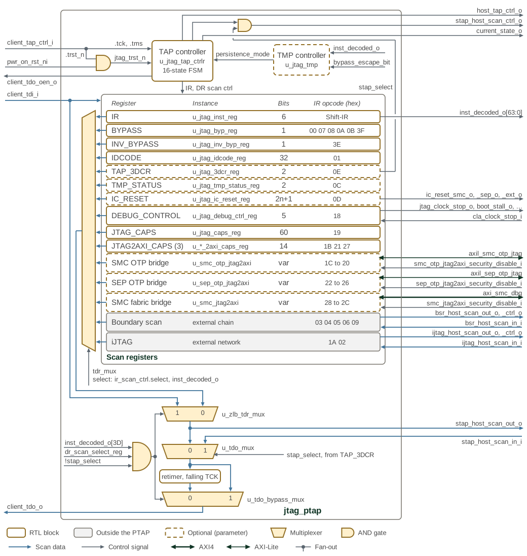
Blue lines carry scan data and grey lines carry control. client_tdi_i feeds the
instruction register and every register in the scan-register group, whose last
column gives the IR opcodes, in hex, that select each register for a DR scan. The
6-bit instruction register captures 6’b000001, resets to IDCODE and decodes its
opcode one-hot onto inst_decoded_o[63:0]. An opcode with no register of its own,
or one whose enable parameter is 0, selects BYPASS. Dashed registers and bridges
are present only when their parameter enables them
(Table 1). The boundary-scan chain and the iJTAG network
lie outside the PTAP: client_tdi_i is forwarded to them, and their returns enter
the TDR multiplexer.
tdr_mux takes the output of every register in the group and the boundary-scan
and iJTAG returns. It selects the instruction register while ir_scan_ctrl.select
is set, and otherwise the register that inst_decoded_o selects. The numbers on
the inputs of each 2:1 multiplexer are the select values that pass them.
u_zlb_tdr_mux passes client_tdi_i instead of tdr_mux during a
ZERO_LENGTH_BYPASS DR scan, and its output also leaves on stap_host_scan_out_o
toward the STAP chain. u_tdo_mux passes the chain return stap_host_scan_in_i
while stap_select, the TAP_3DCR select bit, is set. The retimer registers the
result on the falling TCK edge, and u_tdo_bypass_mux bypasses the retimer during
a ZERO_LENGTH_BYPASS DR scan. Both ZERO_LENGTH_BYPASS multiplexers take their
select from inst_decoded_o[3D] ANDed with dr_scan_select_reg, the DR scan
select registered on the falling TCK edge, and with the inverse of stap_select.
While stap_select is set, ZERO_LENGTH_BYPASS therefore behaves exactly as
BYPASS (Section 3.4.1).
pwr_on_rst_ni is ANDed with the client TRST in u_trst_n_and. The result,
jtag_trst_n, resets the TAP controller and the retimer, and the controller
forwards it with TCK and TMS on host_tap_ctrl_o. The controller also drives the
IR and DR scan controls, ORed together and gated by stap_select, on
stap_host_scan_ctrl_o, so the STAP chain holds its state while the bit is clear.
The TMP controller takes the decoded CLAMP_HOLD, CLAMP_RELEASE and BYPASS
instructions and the TMP_STATUS bypass_escape_bit, and returns persistence_mode
to the TAP controller. The AXI side of each JTAG2AXI bridge runs on clk_i and
rst_n_i and takes the DFT test-mode enable test_en_i; the figure omits all
three. Each bridge has its own *_security_disable_i input
(Table 16).
3.1. Module Hierarchy
Table 1 identifies the PTAP submodules and the conditions under which they are instantiated.
| Module | Purpose | Conditional |
|---|---|---|
|
IEEE 1149.1 TAP controller FSM (16 states, one-hot encoded) |
Always instantiated |
|
6-bit instruction register with 64-wide one-hot decoded output |
Always instantiated |
|
1-bit bypass register (BYPASS instruction) |
Always instantiated |
|
1-bit inverted bypass register (INV_BYPASS instruction) |
Always instantiated |
|
32-bit IDCODE register |
Always instantiated |
|
2-bit 3D Control Register for STAP control |
When |
|
Test Mode Persistence controller |
When |
|
2-bit TMP status register |
When |
|
IC_RESET control register (2*(NumSmcIcReset+NumSepIcReset+NumExtIcReset)+1 bits) |
When any of |
|
5-bit debug control register |
Always instantiated |
|
60-bit capabilities readback register |
Always instantiated |
|
JTAG-to-AXI-Lite bridge for SMC OTP controller |
When |
|
JTAG-to-AXI-Lite bridge for SEP OTP controller |
When |
|
JTAG-to-AXI bridge for SMC system fabric |
When |
3.2. TAP Controller State Machine
The TAP controller implements the IEEE 1149.1 16-state finite state machine using one-hot encoding. Each state is assigned a unique bit position within a 16-bit vector, enabling direct state detection via single-bit comparisons.
Table 2 lists the one-hot encodings and functions of the sixteen TAP-controller states.
| State | Encoding | Description |
|---|---|---|
TEST_LOGIC_RESET |
16’h0001 |
State 0: Reset state, instruction register loads IDCODE |
RUN_TEST_IDLE |
16’h0002 |
State 1: Idle state between operations |
SELECT_DR_SCAN |
16’h0004 |
State 2: Select data register scan path |
CAPTURE_DR |
16’h0008 |
State 3: Capture data into selected DR |
SHIFT_DR |
16’h0010 |
State 4: Shift data through selected DR |
EXIT1_DR |
16’h0020 |
State 5: Exit from shift to either pause or update |
PAUSE_DR |
16’h0040 |
State 6: Pause DR shift operation |
EXIT2_DR |
16’h0080 |
State 7: Exit from pause back to shift or update |
UPDATE_DR |
16’h0100 |
State 8: Update DR from shift register |
SELECT_IR_SCAN |
16’h0200 |
State 9: Select instruction register scan path |
CAPTURE_IR |
16’h0400 |
State 10: Capture data into IR (fixed pattern 6’b000001) |
SHIFT_IR |
16’h0800 |
State 11: Shift data through IR |
EXIT1_IR |
16’h1000 |
State 12: Exit from shift to either pause or update |
PAUSE_IR |
16’h2000 |
State 13: Pause IR shift operation |
EXIT2_IR |
16’h4000 |
State 14: Exit from pause back to shift or update |
UPDATE_IR |
16’h8000 |
State 15: Update IR, decode new instruction |
Five consecutive TCK cycles with TMS high bring the state machine to TEST_LOGIC_RESET from any state, as the IEEE 1149.1 state graph defines. A state register value that is not one of the sixteen one-hot encodings also moves to TEST_LOGIC_RESET on the next rising edge of TCK.
Control signals are generated using a split approach. The update and run-test-idle signals are decoded combinationally from the current state as Moore machine outputs. The capture, shift, test-logic-reset and TDO output enable signals are decoded from the current state and registered on the falling edge of TCK, so they are stable before the next rising edge samples data.
3.3. Reset Hierarchy
The PTAP employs a three-level reset hierarchy to support power-on initialization, JTAG reset, and conditional register preservation.
Table 3 identifies the source and scope of each PTAP reset.
| Reset Signal | Source | Scope |
|---|---|---|
|
|
Primary reset for all JTAG logic, combines power-on and external TRST |
|
Derived from TAP FSM state (asserted when state == TEST_LOGIC_RESET) |
Resets instruction and data registers |
|
|
Channel reset for TMP-aware registers, preserves state when in persistence mode |
The primary reset jtag_trst_n is formed by AND-gating the power-on reset input
with the external TRST signal. This combined reset feeds all JTAG clock domain
logic. The TAP controller derives test_logic_reset from the FSM state, which
normally resets all registers. When Test Mode Persistence is enabled, the
conditional reset chrst_n allows boundary scan and configuration registers to
survive TEST_LOGIC_RESET state transitions while in persistence mode.
3.4. TDR Multiplexer
The PTAP implements an instruction-dependent data register multiplexer. During IR scan operations, the instruction register connects to the scan path. During DR scan operations, the appropriate data register is selected based on the currently decoded instruction. Each test data register has dedicated scan control logic that enables selection only when the corresponding instruction is active and the required feature is enabled.
The scan path supports zero-length bypass through explicit prim_stdmux2
multiplexer cells rather than behavioral multiplexing. This implementation
prevents glitches on scan path selectors during instruction transitions.
STAP selection is implemented as a second-level multiplexer. When the 3DCR register’s select bit is asserted, the STAP chain input replaces the TDR multiplexer output. The STAP scan control signals are generated by OR-combining the instruction register and data register scan controls, enabling STAP operation during both IR and DR scan sequences as required by IEEE 1838. The select bit also gates the select, capture, shift and update strobes of the STAP scan interface, so they stay low while the bit is clear.
3.4.1. Zero-Length Bypass
While the TAP_3DCR STAP-select bit is clear, the ZERO_LENGTH_BYPASS instruction connects TDI directly to TDO without intermediate register stages, providing minimum scan latency for hierarchical JTAG chains. The DR scan adds no bit, and TDO follows TDI combinationally rather than through the retimer.
While the STAP-select bit is set, ZERO_LENGTH_BYPASS behaves exactly as BYPASS. The last stage of the STAP chain shifts on the rising TCK edge, so its return must reach TDO through the falling-edge retimer, and a path that skips the retimer cannot carry it. The bypass register is selected, captures 0 and leads the STAP chain, and TDO is retimed. A DR scan under ZERO_LENGTH_BYPASS is then one bit longer than the STAP chain and matches a DR scan under BYPASS bit for bit.
3.5. TDO Retiming
The TDO output is retimed on the falling edge of TCK as required by IEEE 1149.1
Section 4.5.2. The retiming register ensures that TDO transitions occur at the
same clock edge that samples TDI at the receiving device, maintaining timing
margins across board-level JTAG chains. For zero-length bypass operation with
the TAP_3DCR STAP-select bit clear, the retimer is bypassed using an explicit
prim_stdmux2 cell to minimize scan latency. While the bit is set, TDO is
retimed under every instruction, ZERO_LENGTH_BYPASS included.
3.6. ID Code
The IDCODE instruction accesses a TDR containing device identification information.
Table 4 defines the identification fields shifted out by IDCODE.
| Bits | Field | Access | Description |
|---|---|---|---|
31:28 |
si_rev |
R |
Silicon revision |
27:12 |
part_num |
R |
Chiplet model ID |
11:1 |
mfr_id |
R |
JEDEC-assigned manufacturer ID, encoded into 11 bits |
0 |
marker |
R |
Marker bit, always 1 |
Bits shifted into the IDCODE TDR are ignored. The Programmer’s Guide gives the TDR access sequence for this register.
3.7. Debug Control
The DEBUG_CONTROL instruction accesses a TDR defining general control bits for debug and control of the design.
Table 5 defines the clock-stop and debug-control fields of the DEBUG_CONTROL TDR.
| Bits | Field | Access | Reset | Description |
|---|---|---|---|---|
4 |
cla_clock_stop |
R |
0 |
When set, indicates that a CLA in the chiplet attempted to stop the clocks. Note that the clocks will actually have been stopped only when cla_clock_stop_en is set. |
3 |
jtag_clock_stop |
RW |
0 |
When set, stops all clocks in the chiplet. This is wired to the functional clock gaters on all of the PLLs in the chiplet. This bit is active high. |
2 |
cla_clock_stop_en |
RW |
0 |
When set, enables the CLAs to stop the clocks in the design. This bit indicates that an external debugger is connected and ready to do debug or scan dump operations after the CLA stops the clocks. This bit is intended to protect against unintentional CLA clock stops in the field due to incorrect CLA programming. This bit is active high. |
1 |
boot_stall_ovrd |
RW |
0 |
When set, overrides the boot stall signal to the internals of the part to use the value from boot_stall in this TDR instead. This bit is active high. |
0 |
boot_stall |
RW |
0 |
When boot_stall_override is set, the value in this bit is used for boot stall. This bit is active high: setting to 1 causes boot stall. |
The DEBUG_CONTROL TDR captures bits shifted into its R/W fields and ignores those shifted into its RO fields. The Programmer’s Guide gives the TDR access sequence for this register.
3.8. JTAG Capabilities
The JTAG_CAPS instruction accesses a read-only TDR reporting the DTP version number and general configuration parameters for the DTP.
Table 6 defines the version and configuration fields reported by JTAG_CAPS.
| Bits | Field | Access | Description |
|---|---|---|---|
59:54 |
num_xtrig_int_ct |
R |
The number of internal cross trigger signals. |
53:48 |
num_xtrig_ctp |
R |
The number of Cross Trigger Ports. |
47:44 |
num_xtra_stap |
R |
The number of additional DTP STAP interfaces. |
43 |
stap_io_en |
R |
The STAP interface for chiplet-to-chiplet connectivity is enabled. |
42 |
sep_dbg_en |
R |
The SEP STAP interface enabled. |
41 |
smc_dbg_en |
R |
The SMC JTAG2AXI interface is enabled. |
40:33 |
num_smc_ic_rst |
R |
The number of SMC IC_RESET override ports. |
32:25 |
num_sep_ic_rst |
R |
The number of SEP IC_RESET override ports. |
24:17 |
num_ext_ic_rst |
R |
The number of external IC_RESET override ports. |
16 |
ic_rst_inst_en |
R |
The IC_RESET instruction is enabled. |
15 |
tmp_inst_en |
R |
The TMP controller functionality and instructions are enabled. |
14 |
runbist_inst_en |
R |
The RUNBIST instruction is enabled. |
13 |
highz_inst_en |
R |
The HIGHZ instruction is enabled. |
12 |
clamp_inst_en |
R |
The CLAMP instruction is enabled. |
11 |
intest_inst_en |
R |
The INTEST instruction is enabled. |
10 |
extest_pulse_en |
R |
The EXTEST_PULSE instruction is enabled. |
9 |
extest_train_en |
R |
The EXTEST_TRAIN instruction is enabled. |
8 |
bsr_inst_en |
R |
All mandatory boundary scan instructions are enabled. |
7:0 |
och_ver |
R |
The MAJOR version number of the DTP IP. |
Bits shifted into the JTAG_CAPS TDR are ignored. The Programmer’s Guide gives the TDR access sequence for this register.
3.9. Boundary Scan Support
All boundary scan and BIST instructions defined in IEEE 1149.1 are optionally supported, but support is not enabled by default. RTL parameters are provided to selectively enable support for each instruction. Any disabled instruction has the same behavior as the BYPASS instruction.
Any boundary scan instruction that selects the BSRs shifts their contents out on TDO. The Programmer’s Guide gives the TDR access sequence for these registers.
3.10. BIST Support
The RUNBIST instruction is optionally supported, but support is not enabled by default. An RTL parameter is provided to selectively enable support. Any disabled instruction has the same behavior as the BYPASS instruction.
When the RUNBIST instruction is selected, the iJTAG network is selected as the active scan chain. An iJTAG network control signal indicates that the RUNBIST instruction is active. A designer may also utilize the decoded INST_SELECT signal to trigger the BIST logic for any instructions that they have enabled.
The PTAP adds no Segment Insertion Bit (SIB) or other scan cell to the iJTAG path. TDI is forwarded unchanged to the iJTAG network, and the network’s return is the RUNBIST TDR, so the length and contents of the RUNBIST DR are defined entirely by the iJTAG network attached to the PTAP.
The Programmer’s Guide gives the BIST execution sequence.
In the JTAG Interface Unit, the iJTAG network begins with three SIBs; their bit map and the integrated scan sequence are given in iJTAG Network.
3.11. Test Mode Persistence (TMP) Support
There is optional support for TMP, but support for TMP is disabled by default. An RTL parameter enables support for TMP.
When TMP support is enabled, a TMP controller is included in the PTAP. The TMP controller manages the active-low CH_RESET_N signal. The CH_RESET_N signal is the reset signal for any registers that must retain their state across TLR soft resets, mainly the boundary scan cells. CH_RESET_N asserts whenever the TAP is in the TLR state except when the TMP controller is in the PERSISTENCE_ON state. When the TMP controller is in the PERSISTENCE_ON state, the only events that will assert CH_RESET_N are full power-on-reset (POR) or TRST signal assertion.
When TMP support is disabled, the CLAMP_HOLD, CLAMP_RELEASE, and TMP_STATUS instructions have the same behavior as the BYPASS instruction, and the CH_RESET_N signal always responds to every POR, TRST, or TLR event, i.e. it is an exact copy of the RESET_N signal.
Table 7 defines the bypass-escape and persistence-status bits.
| Bit | Reset | Description |
|---|---|---|
Bypass Escape (bit 0) |
0 |
Whenever this bit is set, the TMP controller will transition to the PERSISTENCE_OFF state when the TAP controller enters the UPDATE_IR state after the BYPASS instruction has been selected. |
TMP Status (bit 1) |
0 on capture |
Capture-DR samples whether the TMP controller is in the Persistence-On state. The update register resets to |
3.12. 3DIC Support
There is optional support for STAP interfaces, and support is enabled by default. An RTL parameter selects the number of STAP interfaces, where a value of 0 disables STAP support.
In order to properly support the IEEE 1838 standard, a chain of STAP interfaces must be inserted at the end of each chiplet’s scan chain. This is done after the IR Select MUX to ensure that both the instruction registers and TDRs from all enabled PTAPs in the scan chain are scannable. As a consequence, the STAPs require dedicated capture, shift, and update control signals that are triggered during both the IR and DR sequences.
The PTAP has a 2-bit 3DCR register that is accessed with the TAP_3DCR instruction. This register provides an option to bypass all STAPs in the scan chain.
Table 8 defines the configuration-hold and STAP-selection bits.
| Bit | Reset | Description |
|---|---|---|
Config Hold |
0 |
When this bit is set, the PTAP TLR state does not reset this TDR, and it will hold its current state until TRST is asserted. |
Select |
0 |
When this bit is unset, the PTAP’s top-level STAP scan interface is completely bypassed: TDO does not come from the STAP chain, and the select, capture, shift and update strobes of the STAP scan interface stay low, so the STAP chain holds its state through every IR and DR scan. |
The select bit takes effect at Update-DR of the scan that writes it. A scan that sets it therefore covers only this register, and the STAP chain joins the scan path from the next IR or DR scan onwards. Software sets the select bit in a TAP_3DCR scan of its own before programming any STAP.
When STAP support is disabled, the TAP_3DCR instruction has the same behavior as the BYPASS instruction, and the STAP scan chain cannot be selected.
3.13. IC_RESET Support
The PTAP provides support for a configurable number of IEEE 1149.1-compliant reset controls. The IC_RESET TDR is composed of three independently-enabled slices:
-
SMC slice (nearest TDI): driven by the
ic_reset_smc_tstruct type and gated byIC_RESET_SMC_ENABLE. Sized from$bits(ic_reset_smc_t). -
SEP slice: driven by the
ic_reset_sep_tstruct type and gated byIC_RESET_SEP_ENABLE. Sized from$bits(ic_reset_sep_t). -
External slice (nearest TDO): driven by the
ic_reset_ext_tstruct type and gated byIC_RESET_EXT_ENABLE. Sized from$bits(ic_reset_ext_t). The instantiator supplies this type; the PTAP does not name the external ports.
Each slice’s struct must contain .ovrd and .val sub-structs of identical
width (checked via an elaboration-time assertion in jtag_ptap). Within
jtag_ic_reset_reg, the reset-enable and reset-control bits are interleaved in
IEEE 1149.1 §17 order: in each port’s pair, reset_enable is nearer TDO and
reset_control nearer TDI, so port n occupies TDR bits 2*n+1 and 2*n+2
(Table 9). jtag_ptap packs the three struct slices into
that interleaved bus and unpacks the outputs back into structured form. The TDR carries the SMC slice closest to TDI, then SEP, then
the external slice, followed by the single reset_hold bit.
The total length is 2 * (NumSmcIcReset + NumSepIcReset + NumExtIcReset) + 1
bits. Each Num*IcReset is half the width of its slice’s struct type,
$bits(ic_reset_*_t) / 2, when the matching IC_RESET_*_ENABLE parameter is
set, and 0 otherwise.
Table 9 defines the reset-control, reset-enable, and bypass fields in the IC_RESET TDR.
| Bits | Field | Access | Reset | Description |
|---|---|---|---|---|
2*n+2 |
reset_control |
RW |
1 |
The controlled, active-low reset value driven while reset_enable is 0 (i.e. while JTAG override is active). |
2*n+1 |
reset_enable |
RW |
1 |
Active-LOW per IEEE 1149.1 §17: 1 (default) ⇒ JTAG override DISABLED (upstream reset passes through); 0 ⇒ JTAG override ENABLED (the port is driven by reset_control). The "enable" in the IEEE name refers to "enabling the controlled reset state", not the override mechanism. |
0 |
reset_hold |
RW |
1 |
When 0, TLR will not reset the reset_enable and reset_control bits. TRST/POR will always reset all bits. |
|
Polarity convention — the TDR field names come from the IEEE 1149.1 §17
specification and use an active-low |
For each of the resets defined in the TDR, the PTAP exposes two logical signals
(grouped into the per-slice jtag_*_reset_ctrl_t structs):
-
ic_reset_ovrd /
.ovrd- Active-high JTAG-override flag (the bit-wise inversion of reset_enable). 1 ⇒ JTAG is driving this reset, 0 ⇒ upstream reset passes through. -
ic_reset_ctrl_n /
.val- Active-low reset value driven when ic_reset_ovrd is asserted (identical to the reset_control TDR bit).
3.14. iJTAG Support
The PTAP provides a scan port for an IEEE 1687-2014-compliant hierarchical iJTAG network. The SELECT_IJTAG instruction is always decoded; no configuration parameter removes it. While it is the current instruction, a DR scan selects the iJTAG network and the network return drives TDO.
3.15. JTAG2AXI Support
3.15.1. *_JTAG2AXI_CAPS
This is a private instruction that accesses a read-only TDR reporting the configuration parameters for the given JTAG2AXI debugging instrument.
Table 10 defines the configuration fields reported by each JTAG2AXI instrument.
| Bits | Field | Access | Description |
|---|---|---|---|
13:12 |
rd_pl_depth |
R |
The depth of the transaction read queue where 0 indicates only a single outstanding transaction allowed at any given time. |
11:10 |
wr_pl_depth |
R |
The depth of the transaction write queue where 0 indicates only a single outstanding transaction allowed at any given time. |
9:7 |
data_size |
R |
The size of AxDATA in powers-of-2 bytes. 0: 1 byte (8 bits) 1: 2 bytes (16 bits) 2: 4 bytes (32 bits) 3: 8 bytes (64 bits) 4: 16 bytes (128 bits) 5: 32 bytes (256 bits) 6: 64 bytes (512 bits) 7: 128 bytes (1024 bits) |
6:1 |
addr_size |
R |
The size of AxADDR in bits. |
0 |
bus_type |
R |
The type of the AXI bus. 0: AXI4 1: AXI4-Lite |
3.15.2. *_AXI_SINGLE_OP
This is a private instruction that generates a single AXI read or write transaction. It provides a mechanism for an external debugger to do sparse reads or writes to nearly any register in the design. Since the entire address must be shifted in for each transaction, this instruction is most useful for sparse accesses. This instruction uses semantics very similar to the RISC-V DTM DMI instruction.
Let D be the AXI data width in bits, A the address width, and S the
scan size-field width: 1 bit for D ⇐ 16, 2 bits for D ⇐ 64, and 3 bits
otherwise. The single-operation TDR has 2 + S + D/8 + D + A bits.
For D=64 and A=51, it has 127 bits.
The size field requests a transfer of 2**size bytes. The AXI protocol does not
allow a transfer wider than the data bus, so the bridge uses the effective size
E = min(size, data_size), where data_size = log2(D/8) is the capability field of
the same name. A size above data_size transfers one full D-bit beat: for
D=32, the 2-bit size field admits 3, and the bridge transfers 4 bytes.
Figure 2 shows the single-operation TDR for a 64-bit data bus and a 51-bit address bus. In this and the following layout figures the most significant bit is on the left, nearest TDI, and bit 0 on the right shifts out to TDO first. The bit range of each field is above it and its width below it; field widths are not drawn to scale.

Table 11 defines the address, data, byte-enable, size, and operation fields.
| Bits | Field | Access | Reset | Description |
|---|---|---|---|---|
(2+S+D/8+D) +: A |
address |
RW |
0 |
Address used for AXI access. In Update-DR the AXI transaction is issued. On a Capture-DR, this field holds the previous value. |
(2+S+D/8) +: D |
data |
RW |
0 |
The data to write on an AXI write during Update-DR. On a Capture-DR, this field contains the data returned from an AXI read if the previous operation was a read, or holds the write data previously used if the previous operation was a write. |
(2+S) +: (D/8) |
wstrb |
RW |
0 |
The byte strobes for a write transaction. This value is driven on WSTRB when the transaction is a write. On a Capture-DR, this field holds the previous value. |
2 +: S |
size |
RW |
0 |
The requested transfer size in powers-of-2 bytes. The effective size |
1:0 |
op |
RW |
0 |
When the debugger writes this field, it has the following meaning: 0: Ignore data and address (nop) Don’t send anything over AXI during Update-DR. This operation should never result in a busy or error response. 1: Read from address (read) 2: Write data to address (write) 3: Reserved When the debugger reads this field, it means the following: 0: The previous operation completed successfully and returned an OKAY status 1: The previous operation completed but failed and returned a SLVERR status 2: The previous operation completed but failed and returned a DECERR or other error status, or a system reset discarded it (see Section 3.15.7). 3: The latest operation was attempted before the previous operation completed; the previous AXI request is still in progress. The operation attempted in this access will be ignored. If a debugger sees this status, it needs to give the target more TCK edges between Update-DR and Capture-DR. The simplest way to do that is to add extra transitions in Run-Test/Idle. |
3.15.3. *_AXI_SERIES_CTRL
This is a private instruction that preloads the start address of a region that will be subsequently read or written using the AXI_SERIES_DATA instruction. It is used when an external debugger wants to either:
-
Read or write a contiguous block of registers or memory.
-
Repeatedly read or write the same location (e.g., polling)
Using the series instructions instead of the AXI_SINGLE_OP instruction is much more time efficient for these use cases.
The pipeline-depth field width P is 1 when FIFO_DEPTH=0, otherwise
$clog2(FIFO_DEPTH+1). The control TDR has 2 + S + P + A + 1 bits.
For D=64, A=51, and FIFO_DEPTH=3, the length is 58 bits.
Figure 3 shows the series-control TDR for 64-bit data, 51-bit addresses, and FIFO_DEPTH=3.

Table 12 defines the control fields used to start and manage a series of AXI accesses.
| Bits | Field | Access | Reset | Description |
|---|---|---|---|---|
(2+S+P+A) |
reset |
RW |
0 |
Reset the pending error flags reported in op. |
(2+S+P) +: A |
address |
RW |
0 |
Address used for AXI access. In Update-DR the AXI transaction is issued. |
(2+S) +: P |
pl_depth |
RW |
0 |
pipeline_depth For write transactions, this sets the number of pending unissued write transactions that can be queued by this block to pl_depth + 1. Setting a non-zero value allows the debugger to queue additional write transactions before the previous ones have been issued. For read transactions, this field sets the number of read responses that this block will pipeline. This allows the debugger to queue multiple reads to targets with long or variable latency while getting read data responses in a deterministic fashion. The first pl_depth + 1 reads will return DEADBEEF marker data. This field can be set to a value between 0 and the (wr/rd)_pl_depth field read from the bridge’s |
2 +: S |
size |
RW |
0 |
The requested transfer size in powers-of-2 bytes. The effective size |
1:0 |
op |
RW |
0 |
When the debugger writes this field, it has the following meaning: 0: Ignore data and address (nop). Don’t do anything on Update-DR for AXI_SERIES_DATA. 1: Read from address (read). Update-DR for AXI_SERIES_DATA causes an AXI read to be performed. 2: Write data to address (write). Update-DR for AXI_SERIES_DATA causes an AXI write to be performed. 3: Reserved; treated as nop. When the debugger reads this field, it means the following: 0: All previous series operations completed successfully and returned an OKAY status. 1: At least one previous series operation completed but failed and returned a SLVERR status. This status is sticky until cleared by AXI_SERIES_CTRL.reset. 2: At least one previous series operation completed but failed and returned a DECERR or other error status, or a system reset discarded a series operation that was in progress or queued (see Section 3.15.7). This status is sticky until cleared by AXI_SERIES_CTRL.reset. Codes 1 and 2 report the first failed series operation since the last AXI_SERIES_CTRL.reset; a later failure does not replace it. The completion status of an AXI_SINGLE_OP operation is reported only through AXI_SINGLE_OP.op and does not change codes 0 to 2. 3: At least one operation was attempted before the previous operation completed. The operations attempted when there was a pending operation in progress were ignored. If a debugger sees this status, it needs to give the target more TCK edges between Update-DR and Capture-DR. The simplest way to do that is to add extra transitions in Run-Test/Idle. This status is sticky until cleared by AXI_SERIES_CTRL.reset. |
3.15.4. *_AXI_SERIES_DATA_INCR
This is a private instruction that does the actual read/write to the address previously specified.
After the access is completed, an internal address register used for the series, which was previously loaded by AXI_SERIES_CTRL, is incremented as follows:
AXI_SERIES_CTRL.address += 2**E
This allows the debugger to load or dump contiguous regions of address space.
Note that this is a variable-length data register. The length is n bits where n = 8*(2**E).
The data field is the logical transfer payload. The bridge places that payload
on the AXI byte lanes selected by the current address and the effective size E,
and Capture-DR returns the payload from those lanes.
The data field is drawn as the payload bytes it holds, with bit 0 aligned across the
four sizes. The incrementing payload layouts for effective sizes E of 0, 1, 2, and 3
are shown in Figure 4,
Figure 5,
Figure 6,
Figure 7, respectively.
Effective size 3 needs a 64-bit data bus, which the last figure assumes.




Table 13 defines the payload shifted through the incrementing data instruction.
| Bits | Field | Access | Reset | Description |
|---|---|---|---|---|
n-1:0 |
data |
RW |
0 |
Data value to read/write. The read data is from the previous read access. |
3.15.5. *_AXI_SERIES_DATA_NO_INCR
This is a private instruction that does the actual read/write to the address previously specified.
Unlike AXI_SERIES_DATA_INCR, this instruction does not change the address in AXI_SERIES_CTRL. This instruction allows the debugger to continue to read or write this same address using additional AXI_SERIES_DATA_NO_INCR instructions. This is useful for repeated polling or triggering.
Note that this is a variable-length data register. The length is n bits where n = 8*(2**E).
The data field is the logical transfer payload. The bridge places that payload
on the AXI byte lanes selected by the current address and the effective size E,
and Capture-DR returns the payload from those lanes.
The non-incrementing data register has the same layout as the incrementing one, so
the same figures apply. The non-incrementing payload layouts for effective sizes E
of 0, 1, 2, and 3 are shown in Figure 8,
Figure 9,
Figure 10,
Figure 11, respectively.
Table 14 defines the payload shifted through the non-incrementing data instruction.
| Bits | Field | Access | Reset | Description |
|---|---|---|---|---|
n-1:0 |
data |
RW |
0 |
Data value to read/write. The read data is from the previous read access. |
3.15.6. *_AXI_SERIES_DATA_WITH_ERROR_STATUS
This is a private instruction that does the actual read/write to the address previously specified.
Unlike AXI_SERIES_DATA_INCR and AXI_SERIES_DATA_NO_INCR, the increment is selectable per transaction and the error status from the previous status is returned. This instruction is used when granular error reporting is desired during a block operation.
Note that this is a variable-length data register. The length is n+1 bits where n = 8*(2**E).
The data field is the logical transfer payload. The bridge places that payload
on the AXI byte lanes selected by the current address and the effective size E,
and Capture-DR returns the payload from those lanes.
The error-status payload layouts for effective sizes E of 0, 1, 2, and 3 are
shown in Figure 12,
Figure 13,
Figure 14,
Figure 15, respectively.
Effective size 3 needs a 64-bit data bus, which the last figure assumes.




Table 15 defines the data payload and the shared increment-control and error-status bit.
| Bits | Field | Access | Reset | Description |
|---|---|---|---|---|
n |
increment/status |
RW |
0 |
The value shifted into this bit indicates whether the address should be incremented after this transaction completes. The value shifted out of this bit indicates whether the previous transaction completed successfully (0 = succeeded, 1 = failed). An AXI result of SLVERR or DECERR, a system reset that discarded the transaction, as well as attempting a new transaction while the previous was still pending will cause the status to be returned as "failed". |
n-1:0 |
data |
RW |
0 |
Data value to read/write. The read data is from the previous read access. |
3.15.7. System Reset Recovery
A system reset resets the AXI side of each JTAG2AXI instrument while its JTAG side keeps running. The instrument recovers without a TAP reset. When the reset reaches its JTAG side, it discards every operation that is in flight or queued: the AXI transaction it was waiting on, series requests not yet issued, and series read data not yet shifted out. The target can still complete a transaction that was already on the AXI bus before the reset reached it, so the debugger must treat a discarded write as having an unknown effect.
After the discard:
-
The SINGLE_OP op field reads 2 if a single operation or an error-status series operation was discarded, and its captured read-data field reads 0. Otherwise both keep their values.
-
The SERIES_CTRL op field reads 2 if a series operation was discarded and it held no earlier series error. Otherwise it keeps its value, including a sticky status of 3. Only AXI_SERIES_CTRL.reset clears it.
-
The SERIES_CTRL address, size, pl_depth and op settings keep their values, but the read pipeline restarts empty. Reprogram SERIES_CTRL before resuming a pipelined series read.
Recovery starts when the system reset asserts and completes within 52 periods of the slower of TCK and the AXI clock after the system reset deasserts. TCK periods count only while the debugger drives TCK, for example with transitions in Run-Test/Idle. An operation shifted in during that time is held and issued once recovery completes, and the SINGLE_OP op field reads 3 until the operation finishes.
3.16. Debug Disable
The PTAP has three per-bridge debug-disable inputs. The JTAG interface unit
synchronizes those bits to TCK and presents them here as ready-to-gate signals.
Each input is active-high: when it is 1, the corresponding jtag2axi instance
blocks AXI transaction generation.
Table 16 maps the three JTAG2AXI bridges to their active-high disable inputs.
| Debug Interface | Disable Input |
|---|---|
SMC Fabric JTAG2AXI |
|
SMC OTP JTAG2AXIL |
|
SEP OTP JTAG2AXIL |
|
4. Interface
4.1. Instruction Encodings
The PTAP uses 6-bit instruction encodings. During the capture phase, the least significant bit (closest to TDO) of the instruction register always presents a 1 to the scan chain, and the next least significant bit presents a 0 as specified by the 1149.1 standard, section 7.2.1. All other bits of the instruction register always return 0s.
Table 17 lists the PTAP instruction encodings and associated register lengths.
| Encoding | Name | Register Size | Description |
|---|---|---|---|
0x00 |
BYPASS |
1 |
IEEE 1149.1, Section 8.4 |
0x01 |
IDCODE |
32 |
IEEE 1149.1, Section 8.13 |
0x02 |
RUNBIST |
BIST |
IEEE 1149.1, Section 8.10 |
0x03 |
SAMPLE_PRELOAD |
BSR |
IEEE 1149.1, Sections 8.6 and 8.7 |
0x04 |
EXTEST |
BSR |
IEEE 1149.1, Section 8.8 |
0x05 |
EXTEST_TRAIN |
BSR |
|
0x06 |
EXTEST_PULSE |
BSR |
|
0x07 |
CLAMP |
1 |
IEEE 1149.1, Section 8.11 |
0x08 |
HIGHZ |
1 |
IEEE 1149.1, Section 8.16 |
0x09 |
INTEST |
BSR |
IEEE 1149.1, Section 8.9 |
0x0A |
CLAMP_HOLD |
2 |
IEEE 1149.1, Section 8.20 |
0x0B |
CLAMP_RELEASE |
2 |
IEEE 1149.1, Section 8.20 |
0x0C |
TMP_STATUS |
2 |
IEEE 1149.1, Section 8.20 |
0x0D |
IC_RESET |
Variable |
IEEE 1149.1, Section 8.21 |
0x0E |
TAP_3DCR |
2 |
IEEE 1838, Section 5.5.1 |
0x18 |
DEBUG_CONTROL |
5 |
Debug and clock stop control |
0x19 |
JTAG_CAPS |
60 |
Capabilities readback |
0x1A |
SELECT_IJTAG |
Variable |
iJTAG network selection |
0x1B |
SMC_OTP_JTAG2AXI_CAPS |
14 |
SMC OTP bridge capabilities readback |
0x1C |
SMC_OTP_AXI_SINGLE_OP |
Variable |
SMC OTP bridge single transaction |
0x1D |
SMC_OTP_AXI_SERIES_CTRL |
Variable |
SMC OTP bridge series control |
0x1E |
SMC_OTP_AXI_SERIES_DATA_INCR |
Variable |
SMC OTP bridge series data, incrementing address |
0x1F |
SMC_OTP_AXI_SERIES_DATA_NO_INCR |
Variable |
SMC OTP bridge series data, fixed address |
0x20 |
SMC_OTP_AXI_SERIES_DATA_WITH_ERROR_STATUS |
Variable |
SMC OTP bridge series data with error status |
0x21 |
SEP_OTP_JTAG2AXI_CAPS |
14 |
SEP OTP bridge capabilities readback |
0x22 |
SEP_OTP_AXI_SINGLE_OP |
Variable |
SEP OTP bridge single transaction |
0x23 |
SEP_OTP_AXI_SERIES_CTRL |
Variable |
SEP OTP bridge series control |
0x24 |
SEP_OTP_AXI_SERIES_DATA_INCR |
Variable |
SEP OTP bridge series data, incrementing address |
0x25 |
SEP_OTP_AXI_SERIES_DATA_NO_INCR |
Variable |
SEP OTP bridge series data, fixed address |
0x26 |
SEP_OTP_AXI_SERIES_DATA_WITH_ERROR_STATUS |
Variable |
SEP OTP bridge series data with error status |
0x27 |
SMC_JTAG2AXI_CAPS |
14 |
SMC fabric bridge capabilities readback |
0x28 |
SMC_AXI_SINGLE_OP |
Variable |
SMC fabric bridge single transaction |
0x29 |
SMC_AXI_SERIES_CTRL |
Variable |
SMC fabric bridge series control |
0x2A |
SMC_AXI_SERIES_DATA_INCR |
Variable |
SMC fabric bridge series data, incrementing address |
0x2B |
SMC_AXI_SERIES_DATA_NO_INCR |
Variable |
SMC fabric bridge series data, fixed address |
0x2C |
SMC_AXI_SERIES_DATA_WITH_ERROR_STATUS |
Variable |
SMC fabric bridge series data with error status |
0x3D |
ZERO_LENGTH_BYPASS |
0, or 1 |
TDI to TDO with no register; BYPASS, with its 1-bit register, while the TAP_3DCR STAP-select bit is set |
0x3E |
INV_BYPASS |
||
0x3F |
BYPASS |
1 |
IEEE 1149.1, Section 8.4 |
The length of each variable-length JTAG2AXI register follows from the bridge’s
address width, data width and pipeline depth, and for the series data registers
from the size last written to *_AXI_SERIES_CTRL. Section 3.15
defines each layout.
NOTE: All instruction encodings not explicitly defined in this table map to the BYPASS instruction.
4.2. Signal Interface
Packed control and bus types remain bundles at the jtag_ptap boundary; their
members are not separate scalar ports.
The parameters and ports of jtag_ptap are listed in jtag_ptap.
4.3. Dependencies
The PTAP depends on the following components:
-
hw/common/ocah_prim— Primitive cells (synchronizers, clock gating) -
hw/ip/jtag/jtag_stap— Secondary TAP (when 3DIC support enabled)